
Data Sheet


KA5L0380R S P S
Preliminary
NOTE:
Pulse test: Pulse width
≤
300
µ
S, duty cycle
≤
2%
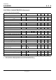
ELECTRICAL CHARACTERISTICS (SFET part)
(Ta=25
°
C unless otherwise specified)
Characteristic Symbol Test condition Min. Typ. Max. Unit
Drain-source breakdown voltage BV
DSS
V
GS
=0V, I
D
=50
µ
A800
−−
V
Zero gate voltage drain current I
DSS
V
DS
=Max., Rating, V
GS
=0V
−−
250
µ
A
V
DS
=0.8Max., Rating,
V
GS
=0V, T
C
=125
°
C
−−
1000
µ
A
Static drain-source on resistance
(note)
R
DS(ON)
V
GS
=10V, I
D
=0.5A
−
45
Ω
Forward transconductance
(note)
gfs V
DS
=50V, I
D
=0.5A 1.5 2.5
−
S
Input capacitance Ciss V
GS
=0V, V
DS
=25V,
f=1MHz
−
779
−
pF
Output capacitance Coss
−
75.6
−
Reverse transfer capacitance Crss
−
24.9
−
Turn on delay time td(on) V
DD
=0.5BV
DSS
, I
D
=1.0A
(MOSFET switching
time are essentially
independent of
operating temperature)
−
40
−
nS
Rise time tr
−
95
−
Turn off delay time td(off)
−
150
−
Fall time tf
−
60
−
Total gate charge
(gate-source+gate-drain)
Qg V
GS
=10V, I
D
=1.0A,
V
DS
=0.5BV
DSS
(MOSFET
switching time are
essentially independent of
operating temperature)
−−
34 nC
Gate-source charge Qgs
−
7.2
−
Gate-drain (Miller) charge Qgd
−
12.1
−
www.onsemi.com
3