
Data Sheet

KA324 / KA324A / KA2902 — Quad Operational Amplifier
© 2002 Fairchild Semiconductor Corporation www.fairchildsemi.com
KA324 / KA324A / KA2902 Rev. 1.1.0 5
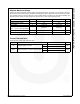
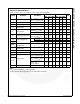
Electrical Characteristics (Continued)
Values are at V
CC
= 5.0 V, V
EE
= GND, unless otherwise specified.
The following specification apply over the range of 0°C ≤ T
A
≤ +70°C for the KA324, and the -40°C ≤ T
A
≤ +85°C for the
KA2902.
Notes:
3. V
CC
= 30 V for KA324, V
CC
= 26 V for KA2902.
4. These parameters, although guaranteed are not 100% tested in production.
Symbol Parameter Conditions
KA324 KA2902
Unit
Min. Typ. Max. Min. Typ. Max.
V
IO
Input Offset Voltage
V
ICM
= 0 V to V
CC
-1.5 V,
V
O(P)
= 1.4 V, R
S
= 0 Ω
(3)
--9.0--10.0mV
ΔV
IO
/ΔT Input Offset Voltage Drift R
S
= 0 Ω
(4)
-7.0- -7.0-μV/
°C
I
IO
Input Offset Current V
CM
= 0 V - - 150 - - 200 nA
ΔI
IO
/ΔT Input Offset Current Drift R
S
= 0 Ω
(4)
-10- -10-pA/
°C
I
BIAS
Input Bias Current V
CM
= 0 V - - 500 - - 500 nA
V
I(R)
Input Common Mode
Voltage Range
(3)
0-
V
CC
-2.0
0-
V
CC
-2.0
V
G
V
Large Signal Voltage Gain
V
CC
= 15 V, R
L
= 2.0 kΩ,
V
O(P)
= 1 V to 11 V
15 - - 15 - - V/mV
V
O(H)
Output Voltage Swing
(3)
R
L
= 2 kΩ 26 - - 22 - - V
R
L
= 10 kΩ 27 28 - 23 24 - V
V
O(L)
V
CC
= 5 V, R
L
= 10 kΩ -520-5100mV
I
SOURCE
Output Current
V
I(+)
= 1 V, V
I(-)
= 0 V,
V
CC
= 15 V, V
O(P)
= 2 V
10 20 - 10 20 - mA
I
SINK
V
I(+)
= 0 V, V
I(-)
= 1 V,
V
CC
= 15 V, V
O(P)
= 2 V
58-58-mA
V
I(DIFF)
Differential Input Voltage - - - V
CC
--V
CC
V