
Data Sheet


©2004 Fairchild Semiconductor Corporation HGTG30N60B3D Rev. B2
Current Turn-On Delay Time t
d(ON)I
IGBT and Diode at T
J
= 150
o
C,
I
CE
= I
C110
,
V
CE
= 0.8 BV
CES
,
V
GE
= 15V,
R
G
= 3Ω,
L = 1mH,
Test Circuit (Figure 19)
-32 - ns
Current Rise Time t
rI
-24 - ns
Current Turn-Off Delay Time t
d(OFF)I
- 275 320 ns
Current Fall Time t
fI
- 90 150 ns
Turn-On Energy E
ON
- 1300 1550 µJ
Turn-Off Energy (Note 3) E
OFF
- 1600 1900 µJ
Diode Forward Voltage V
EC
I
EC
= 30A - 1.95 2.5 V
Diode Reverse Recovery Time t
rr
I
EC
= 1A, dI
EC
/dt = 200A/µs - 32 40 ns
I
EC
= 30A, dI
EC
/dt = 200A/µs - 45 55 ns
Thermal Resistance Junction To Case R
θJC
IGBT - - 0.6
o
C/W
Diode - - 1.3
o
C/W
NOTE:
3. Turn-Off Energy Loss (E
OFF
) is defined as the integral of the instantaneous power loss starting at the trailing edge of the input pulse and
ending at the point where the collector current equals zero (I
CE
= 0A). All devices were tested per JEDEC Standard No. 24-1 Method for
Measurement of Power Device Turn-Off Switching Loss. This test method produces the true total Turn-Off Energy Loss.
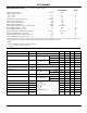
Typical Performance Curves Unless Otherwise Specified
FIGURE 1. DC COLLECTOR CURRENT vs CASE
TEMPERATURE
FIGURE 2. MINIMUM SWITCHING SAFE OPERATING AREA
Electrical Specifications T
C
= 25
o
C, Unless Otherwise Specified (Continued)
PARAMETER SYMBOL TEST CONDITIONS MIN TYP MAX UNITS
T
C
, CASE TEMPERATURE (
o
C)
I
CE
, DC COLLECTOR CURRENT (A)
50
10
0
40
20
30
50
60
V
GE
= 15V
25 75 100 125 150
V
CE
, COLLECTOR TO EMITTER VOLTAGE (V)
125
700
75
0
I
CE
, COLLECTOR TO EMITTER CURRENT (A)
25
50
300 400200100 500 600
100
0
150
175
200
225
T
J
= 150
o
C, R
G
= 3Ω, V
GE
= 15V, L = 100µH
HGTG30N60B3D