
Data Sheet


HGTG20N60A4 Rev. C1
www.fairchildsemi.com3
©2005 Fairchild Semiconductor Corporation
HGTG20N60A4
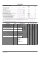
Current Turn-On Delay Time t
d(ON)I
IGBT and Diode at T
J
= 125
o
C
I
CE
= 20A
V
CE
= 390V
V
GE
= 15V
R
G
= 3
L = 500H
Test Circuit (Figure 20)
-1521ns
Current Rise Time t
rI
-1318ns
Current Turn-Off Delay Time t
d(OFF)I
- 105 135 ns
Current Fall Time t
fI
-5573ns
Turn-On Energy (Note 3) E
ON1
- 115 - J
Turn-On Energy (Note 3) E
ON2
- 510 600 J
Turn-Off Energy (Note 2) E
OFF
- 330 500 J
Thermal Resistance Junction To Case R
JC
--0.43
o
C/W
NOTES:
2. Turn-Off Energy Loss (E
OFF
) is defined as the integral of the instantaneous power loss starting at the trailing edge of the input pulse and ending
at the point where the collector current equals zero (I
CE
= 0A). All devices were tested per JEDEC Standard No. 24-1 Method for Measurement
of Power Device Turn-Off Switching Loss. This test method produces the true total Turn-Off Energy Loss.
3. Values for two Turn-On loss conditions are shown for the convenience of the circuit designer. E
ON1
is the turn-on loss of the IGBT only. E
ON2
is the turn-on loss when a typical diode is used in the test circuit and the diode is at the same T
J
as the IGBT. The diode type is specified in
Figure 20.
Electrical Specifications T
J
= 25
o
C, Unless Otherwise Specified (Continued)
PARAMETER SYMBOL TEST CONDITIONS MIN TYP MAX UNIT
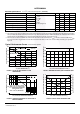
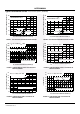
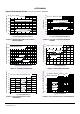
Typical Performance Curves Unless Otherwise Specified
FIGURE 1. DC COLLECTOR CURRENT vs CASE
TEMPERATURE
FIGURE 2. MINIMUM SWITCHING SAFE OPERATING AREA
FIGURE 3. OPERATING FREQUENCY vs COLLECTOR TO
EMITTER CURRENT
FIGURE 4. SHORT CIRCUIT WITHSTAND TIME
T
C
, CASE TEMPERATURE (
o
C)
I
CE
, DC COLLECTOR CURRENT (A)
50
20
0
80
40
60
25 75 100 125 150
100
V
GE
= 15V
PACKAGE LIMIT
DIE CAPABILITY
V
CE
, COLLECTOR TO EMITTER VOLTAGE (V)
700
60
0
I
CE
, COLLECTOR TO EMITTER CURRENT (A)
20
300 400200100 500 600
0
80
100
40
120
T
J
= 150
o
C, R
G
= 3, V
GE
= 15V, L = 100H
f
MAX
, OPERATING FREQUENCY (kHz)
5
I
CE
, COLLECTOR TO EMITTER CURRENT (A)
40
300
5010 20
500
T
J
= 125
o
C, R
G
= 3, L = 500H, V
CE
= 390V
100
4030
f
MAX1
= 0.05 / (t
d(OFF)I
+ t
d(ON)I
)
R
ØJC
= 0.43
o
C/W, SEE NOTES
P
C
= CONDUCTION DISSIPATION
(DUTY FACTOR = 50%)
f
MAX2
= (P
D
- P
C
) / (E
ON2
+ E
OFF
)
T
C
V
GE
15V
75
o
C
V
GE
, GATE TO EMITTER VOLTAGE (V)
I
SC
, PEAK SHORT CIRCUIT CURRENT (A)
t
SC
, SHORT CIRCUIT WITHSTAND TIME (s)
10 11 12 15
0
2
10
100
250
350
45014
13 14
4
6
8
12
150
200
300
400
V
CE
= 390V, R
G
= 3, T
J
= 125
o
C
t
SC
I
SC