
Data Sheet

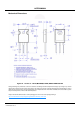

HGTG20N60A4 Rev. C1
www.fairchildsemi.com2
©2005 Fairchild Semiconductor Corporation
HGTG20N60A4
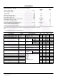
Absolute Maximum Ratings T
C
= 25
o
C, Unless Otherwise Specified
Ratings UNIT
Collector to Emitter Voltage . . . . . . . . . . . . . . . . . . . . . . . . . . . . . . . . . . . . . . . . . . . . . .BV
CES
600 V
Collector Current Continuous
At T
C
= 25
o
C . . . . . . . . . . . . . . . . . . . . . . . . . . . . . . . . . . . . . . . . . . . . . . . . . . . . . . . . . I
C25
70 A
At T
C
= 110
o
C . . . . . . . . . . . . . . . . . . . . . . . . . . . . . . . . . . . . . . . . . . . . . . . . . . . . . . . I
C110
40 A
Collector Current Pulsed (Note 1) . . . . . . . . . . . . . . . . . . . . . . . . . . . . . . . . . . . . . . . . . . . I
CM
280 A
Gate to Emitter Voltage Continuous. . . . . . . . . . . . . . . . . . . . . . . . . . . . . . . . . . . . . . . . .V
GES
20 V
Gate to Emitter Voltage Pulsed . . . . . . . . . . . . . . . . . . . . . . . . . . . . . . . . . . . . . . . . . . . V
GEM
30 V
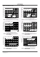
Switching Safe Operating Area at T
J
= 150
o
C (Figure 2) . . . . . . . . . . . . . . . . . . . . . . . SSOA 100A at 600V
Power Dissipation Total at T
C
= 25
o
C . . . . . . . . . . . . . . . . . . . . . . . . . . . . . . . . . . . . . . . . . P
D
290 W
Power Dissipation Derating T
C
> 25
o
C . . . . . . . . . . . . . . . . . . . . . . . . . . . . . . . . . . . . . . . . . . 2.32 W/
o
C
Operating and Storage Junction Temperature Range . . . . . . . . . . . . . . . . . . . . . . . . T
J
, T
STG
-55 to 150
o
C
Maximum Lead Temperature for Soldering
Leads at 0.063in (1.6mm) from Case for 10s. . . . . . . . . . . . . . . . . . . . . . . . . . . . . . . . . . T
L
Package Body for 10s, See Tech Brief 334 . . . . . . . . . . . . . . . . . . . . . . . . . . . . . . . . . T
PKG
300
260
o
C
o
C
CAUTION: Stresses above those listed in “Absolute Maximum Ratings” may cause permanent damage to the device. This is a stress only rating and operation of the
device at these or any other conditions above those indicated in the operational sections of this specification is not implied.
NOTE:
1. Pulse width limited by maximum junction temperature.
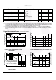
Electrical Specifications T
J
= 25
o
C, Unless Otherwise Specified
PARAMETER SYMBOL TEST CONDITIONS MIN TYP MAX UNIT
Collector to Emitter Breakdown Voltage BV
CES
I
C
= 250A, V
GE
= 0V 600 - - V
Emitter to Collector Breakdown Voltage BV
ECS
I
C
= -10mA, V
GE
= 0V 20 - - V
Collector to Emitter Leakage Current I
CES
V
CE
= 600V T
J
= 25
o
C - - 250 A
T
J
= 125
o
C--2.0mA
Collector to Emitter Saturation Voltage V
CE(SAT)
I
C
= 20A,
V
GE
= 15V
T
J
= 25
o
C-1.82.7V
T
J
= 125
o
C-1.62.0V
Gate to Emitter Threshold Voltage V
GE(TH)
I
C
= 250A, V
CE
= 600V 4.5 5.5 7.0 V
Gate to Emitter Leakage Current I
GES
V
GE
= 20V - - 250 nA
Switching SOA SSOA T
J
= 150
o
C, R
G
= 3V
GE
= 15V
L = 100H, V
CE
= 600V
100 - - A
Gate to Emitter Plateau Voltage V
GEP
I
C
= 20A, V
CE
= 300V - 8.6 - V
On-State Gate Charge Q
g(ON)
I
C
= 20A,
V
CE
= 300V
V
GE
= 15V - 142 162 nC
V
GE
= 20V - 182 210 nC
Current Turn-On Delay Time t
d(ON)I
IGBT and Diode at T
J
= 25
o
C
I
CE
= 20A
V
CE
= 390V
V
GE
=15V
R
G
= 3
L = 500H
Test Circuit (Figure 20)
-15 - ns
Current Rise Time t
rI
-12 - ns
Current Turn-Off Delay Time t
d(OFF)I
-73 - ns
Current Fall Time t
fI
-32 - ns
Turn-On Energy (Note 3) E
ON1
- 105 - J
Turn-On Energy (Note 3) E
ON2
- 280 350 J
Turn-Off Energy (Note 2) E
OFF
- 150 200 J