
Data Sheet


©2005 Fairchild Semiconductor Corporation www.fairchildsemi.com
6N138, 5N139, NCPL2730, HCPL2731 Rev. 1.0.5 2
Single-Channel: 6N138, 6N139 Dual-Channel: HCPL2730, HCPL2731 — Low Input Current High Gain Split Darlington Optocouplers
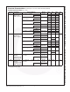
Absolute Maximum Ratings
(T
A
= 25°C unless otherwise specified)
Stresses exceeding the absolute maximum ratings may damage the device. The device may not function or be
operable above the recommended operating conditions and stressing the parts to these levels is not recommended.
In addition, extended exposure to stresses above the recommended operating conditions may affect device reliability.
The absolute maximum ratings are stress ratings only.
Symbol Parameter Value Units
T
STG
Storage Temperature -55 to +125 °C
T
OPR
Operating Temperature -40 to +85 °C
T
SOL
Lead Solder Temperature (Wave solder only. See recommended reflow profile
graph for SMD mounting)
260 for 10 sec °C
EMITTER
I
F
(avg) DC/Average Forward Input Current Each Channel 20 mA
I
F
(pk) Peak Forward Input Current (50% duty cycle, 1 ms P.W.) Each Channel 40 mA
I
F
(trans) Peak Transient Input Current - (
≤
1µs P.W., 300 pps) 1.0 A
V
R
Reverse Input Voltage Each Channel 5 V
P
D
Input Power Dissipation Each Channel 35 mW
DETECTOR
I
O
(avg) Average Output Current Each Channel 60 mA
V
ER
Emitter-Base Reverse Voltage 6N138 and 6N139 0.5 V
V
CC
, V
O
Supply Voltage, Output Voltage 6N138, HCPL2730 -0.5 to 7 V
6N139, HCPL2731 -0.5 to 18
P
O
Output Power Dissipation Each Channel 100 mW