
Data Sheet


©2007 Fairchild Semiconductor Corporation www.fairchildsemi.com
4N38M, H11D1M, H11D3M, MOC8204M Rev. 1.0.7 3
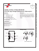
4N38M, H11D1M, H11D3M, MOC8204M — 6-Pin DIP High Voltage Phototransistor Optocouplers
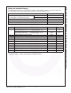
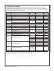
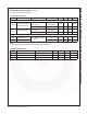
Absolute Maximum Ratings
Stresses exceeding the absolute maximum ratings may damage the device. The device may not function or be
operable above the recommended operating conditions and stressing the parts to these levels is not recommended.
In addition, extended exposure to stresses above the recommended operating conditions may affect device reliability.
The absolute maximum ratings are stress ratings only.
Note:
2. Parameters meet or exceed JEDEC registered data (for 4N38M only).
Symbol Parameter Device Value Unit
TOTAL DEVICE
T
STG
Storage Temperature All -40 to +125 °C
T
OPR
Operating Temperature All -40 to +100 °C
T
J
Junction Temperature All -40 to +125 ºC
T
SOL
Lead Solder Temperature All 260 for 10 seconds °C
P
D
Total Device Power Dissipation @ T
A
= 25°C
All
420 mW
Derate Above 25°C 3.5 mW/°C
EMITTER
I
F
Forward DC Current
(2)
All 80 mA
V
R
Reverse Input Voltage
(2)
All 6.0 V
I
F
(pk)
Forward Current – Peak (1 µs pulse, 300pps)
(2)
All 3.0 A
P
D
LED Power Dissipation @ T
A
= 25°C
(2)
All
120 mW
Derate Above 25°C 1.41 mW/°C
DETECTOR
P
D
Power Dissipation @ T
A
= 25°C
All
300 mW
Derate linearly above 25°C 4.0 mW/°C
V
CEO
Collector to Emitter Voltage
(2)
MOC8204M 400 V
H11D1M 300 V
H11D3M 200 V
4N38M 80 V
V
CBO
Collector Base Voltage
(2)
MOC8204M 400 V
H11D1M 300 V
H11D3M 200 V
4N38M 80 V
V
ECO
Emitter to Collector Voltage
(2)
H11D1M,
H11D3M,
MOC8204M
7V
I
C
Collector Current (Continuous) All 100 mA