
Data Sheet


©2000 Fairchild Semiconductor Corporation www.fairchildsemi.com
H11A1M Rev. 1.1 3
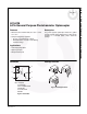
H11A1M — 6-Pin General Purpose Phototransistor Optocoupler
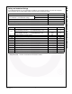
Absolute Maximum Ratings
Stresses exceeding the absolute maximum ratings may damage the device. The device may not function or be
operable above the recommended operating conditions and stressing the parts to these levels is not recommended.
In addition, extended exposure to stresses above the recommended operating conditions may affect device reliability.
The absolute maximum ratings are stress ratings only. T
A
= 25°C unless otherwise specified.
Symbol Parameter Value Unit
TOTAL DEVICE
T
STG
Storage Temperature -40 to +125 °C
T
OPR
Operating Temperature -40 to +100 °C
T
J
Junction Temperature -40 to +125 ºC
T
SOL
Lead Solder Temperature 260 for 10 seconds °C
P
D
Total Device Power Dissipation @ T
A
= 25°C 270 mW
Derate Above 25°C 2.94 mW/°C
EMITTER
I
F
DC/Average Forward Input Current 60 mA
V
R
Reverse Input Voltage 6 V
I
F
(pk) Forward Current – Peak (300 µs, 2% Duty Cycle) 3 A
P
D
LED Power Dissipation @ T
A
= 25°C 120 mW
Derate Above 25°C 1.41 mW/°C
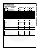
DETECTOR
V
CEO
Collector-to-Emitter Voltage 30 V
V
CBO
Collector-to-Base Voltage 70 V
V
ECO
Emitter-to-Collector Voltage 7 V
P
D
Detector Power Dissipation @ T
A
= 25°C 150 mW
Derate Above 25°C 1.76 mW/°C