
Data Sheet
© 2011 Fairchild Semiconductor Corporation www.fairchildsemi.com
FT3001 • Rev. 1.0.4 3
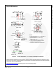
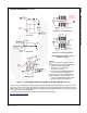
FT3001 — Reset Timer with Configurable Delay
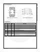
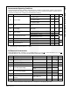
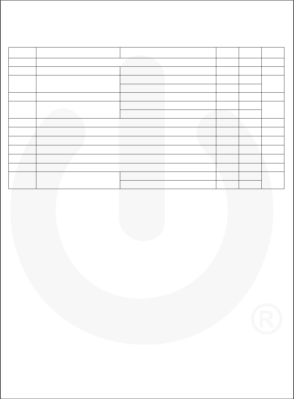
Absolute Maximum Ratings
Stresses exceeding the absolute maximum ratings may damage the device. The device may not function or be
operable above the recommended operating conditions and stressing the parts to these levels is not recommended.
In addition, extended exposure to stresses above the recommended operating conditions may affect device reliability.
The absolute maximum ratings are stress ratings only.
Symbol Parameter Condition Min. Max. Unit
V
CC
Supply Voltage -0.5 7.0 V
V
IN
DC Input Voltage /SR0, /SR1, TRIG, DSR0 -0.5 7.0 V
V
OUT
Output Voltage
(1)
/RST1, RST2 HIGH or LOW -0.5 V
CC
+0.5
V
/RST1, RST2, V
CC
=0 V -0.5 7.0
I
IK
DC Input Diode Current V
IN
< 0 V -50 mA
I
OK
DC Output Diode Current
V
OUT
< 0 V -50
mA
V
OUT
> V
CC
+50
I
OH
/I
OL
DC Output Source/Sink Current -50 +50 mA
I
CC
DC V
CC
or Ground Current per Supply Pin
100
mA
T
STG
Storage Temperature Range -65 +150
C
V
CC
Junction Temperature Under Bias +150
C
V
IN
Junction Lead Temperature, Soldering 10 Seconds +260
C
P
D
Power Dissipation 5 mW
ESD Electrostatic Discharge Capability
Human Body Model, JESD22-A114 4
kV
Charged Device Model, JESD22-C101 2
Note:
1. I
O
absolute maximum rating must be observed.