
Data Sheet
© 2011 Fairchild Semiconductor Corporation www.fairchildsemi.com
FT3001 • Rev. 1.0.4 2
FT3001 — Reset Timer with Configurable Delay
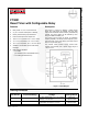
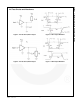
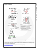
Pin Configurations
10
4
8
3
9
5
2 6
7
1
RST2 DSR1 V
CC
GND
/SR1
/RST1 NC DSR0
/SR0
TRIG
Figure 2. UMLP (Top Through View) Figure 3. MLP (Top Through View)
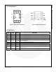
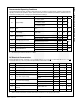
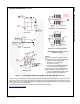
Pin Definitions
UMLP
Pin#
MLP
Pin#
Name Description
1 2 GND Ground
2 3 /SR1 Secondary Reset Input, Active LOW
3 4 /RST1 Open-Drain Output, Active LOW
4 NC No Connect
5
5
DSR0
Delay Selection Input (Must be tied directly to GND or V
CC
; do not use pull-up or
pull-down resistors.)
6 6 TRIG Test Pin; tied to ground in normal use
7 7 /SR0 Primary Reset Input, Active LOW
8 8 V
CC
Power Supply
9
DSR1
Delay Selection Input (Must be tied directly to GND or V
CC
; do not use pull-up or
pull-down resistors.)
10 1 RST2 Push-Pull Output, Active HIGH