
Data Sheet

© 2011 Fairchild Semiconductor Corporation www.fairchildsemi.com
FT3001 • Rev. 1.0.4 9
FT3001 — Reset Timer with Configurable Delay
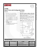
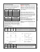
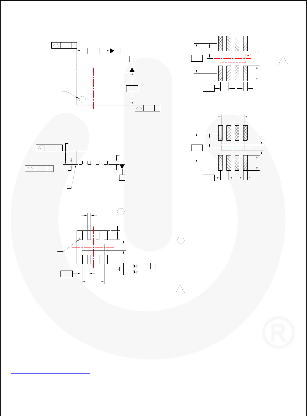
Physical Dimensions (Continued)
BOTTOM VIEW
SIDE VIEW
TOP VIEW
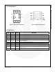
NOTES:
A. PACKAGE CONFORMS TO JEDEC MO-229,
VARIATION W2020D EXCEPT WHERE NOTED.
B. DIMENSIONS ARE IN MILLIMETERS.
C. DIMENSIONS AND TOLERANCES
PER ASME Y14.5M, 1994.
D. LAND PATTERN RECOMMENDATION BASED
ON PCB MATRIX CALCULATOR V2009.
E. IF CENTER PAD IS NOT SOLDERED TO, NO
EXPOSED METAL IS ALLOWED IN THE TOP
LAYER OF THE BOARD IN THE AREA SHOWN.
F. DRAWING FILENAME: MKT-MLP08Rrev2.
0.05
0.00
0.80 MAX
0.10
C
0.08
C
(0.20)
C
SEATING
PLANE
PIN1
IDENT
2.00
2.00
A
B
2X
2X
0.10 C
0.10 C
8
5
1
4
0.10 CAB
0.05
C
PIN 1
IDENT
0.50
0.65
0.45
0.25
0.15
8X
8X
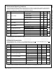
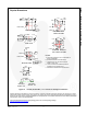
RECOMMENDED LAND PATTERN
(NSMD PAD TYPE)
OPTION #1: NO CENTER PAD
(0.25)
(0.90)
1.80
0.50
8X
8X
OPTION #2: WITH CENTER PAD
E
TOP LAYER
CU KEEP
OUT AREA
0.90
(1.35)
A
(0.25)
(0.90)
1.80
0.50
8X
8X
0.90
(0.35)
1.35 MAX
0.40 MAX
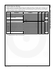
Figure 11. 8-Lead, Molded Leadless Package (MLP), Dual JEDEC, MO-229 2.0 x 2.0 mm
Package drawings are provided as a service to customers considering Fairchild components. Drawings may change in any manner
without notice. Please note the revision and/or date on the drawing and contact a Fairchild Semiconductor representative to verify or
obtain the most recent revision. Package specifications do not expand the terms of Fairchild’s worldwide terms and conditions, specifically the
warranty therein, which covers Fairchild products.
Always visit Fairchild Semiconductor’s online packaging area for the most recent package drawings:
http://www.fairchildsemi.com/packaging/
.