
Data Sheet

© 2007 Fairchild Semiconductor Corporation www.fairchildsemi.com
FSQ0365, FSQ0265, FSQ0165, FSQ321 • Rev. 1.0.6 12
FSQ0365/0265/0165/321 — Green Mode Fairchild Power Switch (FPS™) for Valley Switching Converter
Functional Description
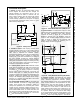
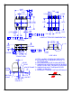
1. Startup: At startup, an internal high-voltage current
source supplies the internal bias and charges the
external capacitor (C
a
) connected to the V
CC
pin, as
illustrated in Figure 20. When V
CC
reaches 12V, the
FPS™ begins switching and the internal high-voltage
current source is disabled. The FPS continues its
normal switching operation and the power is supplied
from the auxiliary transformer winding unless V
CC
goes
below the stop voltage of 8V.
8V/12V
V
ref
Internal
Bias
V
CC
V
str
I
CH
V
CC
good
V
DC
C
a
FSQ0365RN Rev.00
2 5
Figure 20. Startup Circuit
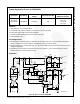
2. Feedback Control: FPS employs Current Mode
control, as shown in Figure 21. An opto-coupler (such as
FOD817A) and shunt regulator (such as KA431) are
often used to implement the feedback network.
Comparing the feedback voltage with the voltage across
the R
SENSE
resistor makes it possible to control the
switching duty cycle. When the reference pin voltage of
the shunt regulator exceeds the internal reference
voltage of 2.5V, the opto-coupler LED current increases,
pulling down the feedback voltage and reducing the duty
cycle. This event typically occurs when input voltage is
increased or output load is decreased.
2.1 Pulse-by-Pulse Current Limit: Because Current
Mode control is employed, the peak current through the
SenseFET is limited by the inverting input of PWM
comparator (V
FB
*), as shown in Figure 21. Assuming
that the 0.9mA current source flows only through the
internal resistor (3R + R = 2.8kΩ), the cathode voltage
of diode D2 is about 2.5V. Since D1 is blocked when the
feedback voltage (V
FB
) exceeds 2.5V, the maximum
voltage of the cathode of D2 is clamped at this voltage,
clamping V
FB
*. Therefore, the peak value of the current
through the SenseFET is limited.
2.2 Leading-Edge Blanking (LEB): At the instant the
internal SenseFET is turned on, a high-current spike
usually occurs through the SenseFET, caused by
primary-side capacitance and secondary-side rectifier
reverse recovery. Excessive voltage across the R
sense
resistor would lead to incorrect feedback operation in the
Current Mode PWM control. To counter this effect, the
FPS employs a leading-edge blanking (LEB) circuit. This
circuit inhibits the PWM comparator for a short time
(t
LEB
) after the SenseFET is turned on.
3
OSC
V
CC
V
ref
I
delay
I
FB
V
SD
R
3R
Gate
driver
OLP
D1 D2
+
V
FB
*
-
V
FB
KA431
C
B
V
O
FOD817A
R
sense
SenseFET
FSQ0365RN Rev. 00
Figure 21. Pulse-Width-Modulation (PWM) Circuit
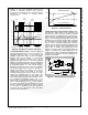
3. Synchronization: The FSQ-series employs a valley
switching technique to minimize the switching noise and
loss. The basic waveforms of the valley switching
converter are shown in Figure 22. To minimize the
MOSFET's switching loss, the MOSFET should be
turned on when the drain voltage reaches its minimum
value, as shown in Figure 22. The minimum drain
voltage is indirectly detected by monitoring the V
CC
winding voltage, as shown in Figure 22.
V
DC
V
RO
V
RO
V
ds
t
F
0.7V
V
sync
300ns Delay
0.2V
ONON
V
ovp
(6V)
FSQ0365RN Rev.00
MOSFET Gate
Figure 22. Valley Resonant Switching Waveforms
4. Protection Circuits: The FSQ-series has several
self-protective functions, such as Overload Protection
(OLP), Abnormal Over-Current protection (AOCP),
Over-Voltage Protection (OVP), and Thermal Shutdown
(TSD). All the protections are implemented as Auto-
Restart Mode. Once the fault condition is detected,
switching is terminated and the SenseFET remains off.
This causes V
CC
to fall. When V
CC
falls down to the
Under-Voltage Lockout (UVLO) stop voltage of 8V, the
protection is reset and the startup circuit charges the
V
CC
capacitor. When the V
CC
reaches the start voltage
of 12V, the FSQ-series resumes normal operation. If the
fault condition is not removed, the SenseFET remains
off and V
CC
drops to stop voltage again. In this manner,