
Data Sheet


© 2011 Fairchild Semiconductor Corporation www.fairchildsemi.com
FSL206MR • Rev. 1.0.5 4
FSL206MR — Green Mode Fairchild Power Switch (FPS™)
Absolute Maximum Ratings
Stresses exceeding the absolute maximum ratings may damage the device. The device may not function or be
operable above the recommended operating conditions and stressing the parts to these levels is not recommended.
In addition, extended exposure to stresses above the recommended operating conditions may affect device reliability.
The absolute maximum ratings are stress ratings only. T
A
= 25°C unless otherwise specified.
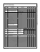
Symbol Parameter Min. Max. Unit
V
STR
V
STR
Pin Voltage -0.3 650.0 V
V
DS
Drain Pin Voltage -0.3 650.0 V
V
CC
Supply Voltage 26 V
V
LS
LS Pin Voltage -0.3
Internally Clamped
Voltage
(4)
V
V
FB
Feedback Voltage Range -0.3
Internally Clamped
Voltage
(4)
V
I
DM
Drain Current Pulsed
(5)
1.5 A
E
AS
Single-Pulsed Avalanche Energy
(6)
11 mJ
P
D
Total Power Dissipation 1.3 W
T
J
Operating Junction Temperature -40 +150 °C
T
A
Operating Ambient Temperature -40 +125 °C
T
STG
Storage Temperature -55 +150 °C
ESD
Human Body Model, JESD22-A114 4
KV
Charged Device Model, JESD22-C101 2
Notes:
4. V
FB
is clamped by internal clamping diode (13V I
CLAMP_MAX
< 100A). After shutdown, before V
CC
reaching V
STOP
,
V
SD
< V
FB
< V
CC
.
5. Repetitive rating: pulse-width limited by maximum junction temperature.
6. L=21mH, starting T
J
=25°C.
Thermal Impedance
T
A
=25°C unless otherwise specified.
Symbol Parameter Value Unit
JA
Junction-to-Ambient Thermal Impedance
(7)
93 °C/W
Notes:
7. JEDEC recommended environment, JESD51-2 and test board, JESD51-10 with minimum land pattern for 8DIP
and JESD51-3 with minimum land pattern for 8LSOP.