
Data Sheet


© 2011 Fairchild Semiconductor Corporation www.fairchildsemi.com
FSL206MR • Rev. 1.0.5 3
FSL206MR — Green Mode Fairchild Power Switch (FPS™)
Pin Configuration
Figure 3. Pin Configuration
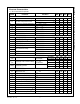
Pin Definitions
Pin # Name Description
1 GND
Ground. SenseFET source terminal on primary side and internal control ground.
2 V
CC
Positive Supply Voltage Input. Although connected to an auxiliary transformer winding,
current is supplied from pin 5 (V
STR
) via an internal switch during startup (see Internal Block
Diagram section). It is not until V
CC
reaches the UVLO upper threshold (8V) that the internal
startup switch opens and device power is supplied via the auxiliary transformer winding.
3 V
FB
Feedback Voltage. Non-inverting input to the PWM comparator, with a 0.11mA current source
connected internally and a capacitor and opto-coupler typically connected externally. There is a
delay while charging external capacitor C
FB
from 2.4V to 5V using an internal 2.7A current
source. This delay prevents false triggering under transient conditions, but allows the protection
mechanism to operate under true overload conditions.
4 LS
Line Sense Pin. This pin is used to protect the device when the input voltage is lower than the
rated input voltage range. If this pin is not used, connect to ground.
5 V
STR
Startup. Connected to the rectified AC line voltage source. At startup, the internal switch
supplies internal bias and charges an external storage capacitor placed between the V
CC
pin
and ground. Once V
CC
reaches 8V, all internal blocks are activated. After that, the internal high-
voltage regulator (HV REG) turns on and off irregularly to maintain V
CC
at 7.8V.
6, 7, 8 Drain
Drain. Designed to connect directly to the primary lead of the transformer and capable of
switching a maximum of 650V. Minimizing the length of the trace connecting these pins to the
transformer decreases leakage inductance.