
Data Sheet


© 2009 Fairchild Semiconductor Corporation www.fairchildsemi.com
FSGM0765R • Rev. 1.0.2 4
FSGM0765R — Green-Mode Fairchild Power Switch (FPS™)
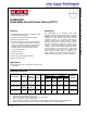
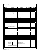
Absolute Maximum Ratings
Stresses exceeding the absolute maximum ratings may damage the device. The device may not function or be
operable above the recommended operating conditions and stressing the parts to these levels is not recommended.
In addition, extended exposure to stresses above the recommended operating conditions may affect device
reliability. The absolute maximum ratings are stress ratings only.
Symbol Parameter Min. Max. Unit
V
STR
V
STR
Pin Voltage 650 V
V
DS
Drain Pin Voltage 650 V
V
CC
V
CC
Pin Voltage 26 V
V
FB
Feedback Pin Voltage
-0.3 12.0 V
I
DM
Drain Current Pulsed 12.8 A
I
DS
Continuous Switching Drain Current
(6)
T
C
=+25°C
6.4 A
T
C
=+100°C
4.0 A
E
AS
Single Pulsed Avalanche Energy
(7)
390 mJ
P
D
Total Power Dissipation (T
C
=+25°C)
(8)
45 W
T
J
Maximum Junction Temperature
+150
°C
Operating Junction Temperature
(9)
-40 +125
°C
T
STG
Storage Temperature
-55 +150
°C
V
ISO
Minimum Isolation Voltage
(10)
2.5 V
ESD
Electrostatic
Discharge Capability
Human Body Model, JESD22-A114 2
kV
Charged Device Model, JESD22-C101 2
Notes:
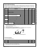
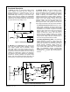
6. Repetitive peak switching current when the inductive load is assumed: Limited by maximum duty (D
MAX
=0.75)
and junction temperature (see Figure 4).
7. L=70mH, starting T
J
=+25°C.
8. Infinite cooling condition (refer to the SEMI G30-88).
9. Although this parameter guarantees IC operation, it does not guarantee all electrical characteristics.
10. The voltage between the package back side and the lead is guaranteed.
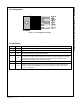
Figure 4. Repetitive Peak Switching Current
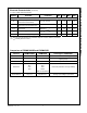
Thermal Impedance
T
A
=25°C unless otherwise specified.
Symbol Parameter Value Unit
JA
Junction-to-Ambient Thermal Impedance
(11)
62.5 °C/W
JC
Junction-to-Case Thermal Impedance
(12)
3 °C/W
Notes:
11. Infinite cooling condition (refer to the SEMI G30-88).
12. Free standing with no heat-sink under natural convection.