
Data Sheet

© 2011 Fairchild Semiconductor Corporation www.fairchildsemi.com
FSFR1800 / FSFR1700-HS • Rev.1.0.1 3
FSFR-HS Series — Advanced Fairchild Power Switch (FPS™) for Half-Bridge Resonant Converter
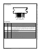
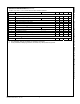
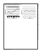
Pin Configuration
Figure 3. Package Diagram
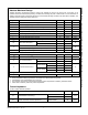
Pin Definitions
Pin # Name Description
1 DL This is the drain of the high-side MOSFET, typically connected to the input DC link voltage.
2 LS This is the line-sensing pin for the input voltage Under-Voltage Lockout (UVLO).
3 RT
This pin is used for controlling the switching frequency in normal operation. When any
protections are triggered, the internal Auto/Restart (A/R) circuit starts to sense the voltage on
the pin, which is discharged naturally by external resistance. The IC can be operated with
A/R when the voltage decreases 0.1 V. Typically, an opto-coupler is connected to control the
switching frequency for the output voltage regulation and resistors for setting minimum /
maximum operating frequency.
4 CS
This pin senses the current flowing through the low-side MOSFET. Typically, negative
voltage is applied to this pin.
5 SG This pin is the ground of the control part.
6 PG This pin is the power ground. This pin is connected to the source of the low-side MOSFET.
7 LV
CC
This pin is the supply voltage of the control IC.
8 NC No connection
9 HV
CC
This is the supply voltage of the high-side gate-drive circuit.
10 CTR This is the drain of the low-side MOSFET. Typically, a transformer is connected to this pin.