
Data Sheet


FSBB15CH60C Motion SPM® 3 Series
6 www.fairchildsemi.com©2008 Fairchild Semiconductor Corporation
FSBB15CH60C Rev. 1.6
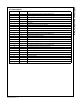
Electrical Characteristics (T
J
= 25°C, unless otherwise specified.)
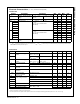
Inverter Part
Symbol Parameter Conditions Min. Typ. Max. Unit
V
CE(SAT)
Collector - Emitter Saturation
Voltage
V
CC
= V
BS
= 15 V
V
IN
= 5 V
I
C
= 15 A, T
J
= 25°C - - 2.0 V
V
F
FWDi Forward Voltage V
IN
= 0 V I
F
= 15 A, T
J
= 25°C - - 2.2 V
HS t
ON
Switching Times V
PN
= 300 V, V
CC
= V
BS
= 15 V
I
C
= 15 A
V
IN
= 0 V ↔ 5 V, Inductive Load
(2nd Note 3)
- 0.80 - μs
t
C(ON)
- 0.20 - μs
t
OFF
- 0.40 - μs
t
C(OFF)
- 0.10 - μs
t
rr
- 0.10 - μs
LS t
ON
V
PN
= 300 V, V
CC
= V
BS
= 15 V
I
C
= 15 A
V
IN
= 0 V ↔ 5 V, Inductive Load
(2nd Note 3)
- 0.50 - μs
t
C(ON)
- 0.25 - μs
t
OFF
- 0.35 - μs
t
C(OFF)
- 0.10 - μs
t
rr
- 0.10 - μs
I
CES
Collector - Emitter Leakage
Current
V
CE
= V
CES
- - 1 mA
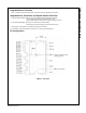
2nd Notes:
3. t
ON
and t
OFF
include the propagation delay time of the internal drive IC. t
C(ON)
and t
C(OFF)
are the switching time of IGBT itself under the given gate driving condition internally.
For the detailed information, please see Figure 4.
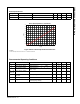
Control Part
Symbol Parameter Conditions Min. Typ. Max. Unit
I
QCCL
Quiescent V
CC
Supply
Current
V
CC
= 15 V
IN
(UL, VL, WL)
= 0 V
V
CC(L)
- COM - - 23 mA
I
QCCH
V
CC
= 15 V
IN
(UH, VH, WH)
= 0 V
V
CC(H)
- COM - - 600 μA
I
QBS
Quiescent V
BS
Supply
Current
V
BS
= 15 V
IN
(UH, VH, WH)
= 0 V
V
B(U)
- V
S(U)
, V
B(V)
- V
S(V)
,
V
B(W)
- V
S(W)
- - 500 μA
V
FOH
Fault Output Voltage V
SC
= 0 V, V
FO
Circuit: 4.7 kΩ to 5 V Pull-up 4.5 - - V
V
FOL
V
SC
= 1 V, V
FO
Circuit: 4.7 kΩ to 5 V Pull-up - - 0.8 V
V
SC(ref)
Short-Circuit Current
Trip Level
V
CC
= 15 V (2nd Note 4) 0.45 0.50 0.55 V
TSD Over-Temperature
Protection
T
emperature at LVIC - 160 - °C
ΔTSD Over-Temperature
Protection Hyster
isis
Temperature at LVIC - 5 - °C
UV
CCD
Supply Circuit
Under-Voltage Protection
Detection Level 10.7 11.9 13.0 V
UV
CCR
Reset Level 11.2 12.4 13.4 V
UV
BSD
Detection Level 10 11 12 V
UV
BSR
Reset Level 10.5 11.5 12.5 V
t
FOD
Fault-Out Pulse Width C
FOD
= 33 nF (2nd Note 5) 1.0 1.8 - ms
V
IN(ON)
ON Threshold Voltage Applied between IN
(UH)
, IN
(VH)
, IN
(WH)
, IN
(UL)
,
IN
(VL)
, IN
(WL)
- COM
2.8 - - V
V
IN(OFF)
OFF Threshold Voltage - - 0.8 V
2nd Notes:
4. Short-circuit protection is functioning only at the low-sides.
5. The fault-out pulse width t
FOD
depends on the capacitance value of C
FOD
according to the following approximate equation: C
FOD
= 18.3 x 10
-6
x t
FOD
[F]