
Data Sheet

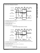


MCU
SPM
COM
+5 V
,,
IN
(UL)
IN
(VL)
IN
(WL)
,,
IN
(UH)
IN
(VH)
IN
(WH)
V
FO
1 nF
C
PF
= 1 nF
R
PF
= 4.7 ㏀
100 Ω
100 Ω
1 nF 1 nF
100 Ω
FSBB15CH60C Motion SPM® 3 Series
12 www.fairchildsemi.com©2008 Fairchild Semiconductor Corporation
FSBB15CH60C Rev. 1.6
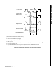
Figure 11. Recommended MCU I/O Interface Circuit
15 V
22 µF
0.1 µF
1000 µF1 µF
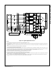
One-Leg Diagram of
Motion SPM 3 Product
Inverter
Output
P
N
These values depend on PWM control algorithm.
Vcc
IN
COM
VB
HO
VS
Vcc
IN
COM
OUT
V
SL
3rd Notes:
1. RC coupling at each input might change depending on the PWM control scheme in the application and the wiring impedance of the application’s printed circuit board. The input
signal section of the Motion SPM
®
3 product integrates a 5 kΩ (typ.) pull-down resistor. Therefore, when using an external filtering resistor, please pay attention to the signal
voltage drop at input terminal.
2. The logic input works with standard CMOS or LSTTL outputs.
Figure 12. Recommended Bootstrap Operation Circuit and Parameters
3rd Notes:
3. The ceramic capacitor placed between V
CC
- COM should be over 1 μF and mounted as close to the pins of the Motion SPM 3 product as possible.