
Data Sheet

www.onsemi.com
6
FSA642 — Low-Power, Three-Port, High-Speed MIPI Switch
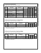
AC Electrical Characteristics
All values are at R
L
=50Ω and R
S
=50Ω and all typical values are V
CC
=2.775V at T
A
=25°C unless otherw ise specified.
Symbol
Parameter
Conditions
V
CC
(V)
T
A
=-40ºC to +85ºC
Units
Min.
Typ.
Max.
O
IRR
Off Isolation
(7)
f=100 MHz, R
T
=50 Ω
Figure 14
2.775
-35
dB
Xtalk
Non-Adjacent Channel
Crosstalk
(7)
f=100 MHz, R
T
=50 Ω
Figure 15
2.775
-55
dB
BW
-3 db Bandw idth
(7)
C
L
=0 pF, R
T
=50 Ω
Figure 13
2.775
1.0
GHz
t
ON
Turn-On Time
SEL, /OE to Output
C
L
=5 pF, V
SW
=1.2 V
Figure 6, Figure 7
2.650 to 2.775
20
37
ns
t
OFF
Turn-Off Time
SEL, /OE to Output
C
L
=5 pF, V
SW
=1.2 V
Figure 6, Figure 7
2.650 to 2.775
15
27
ns
t
PD
Propagation Delay
(7)
C
L
=5 pF
Figure 6, Figure 8
2.775
0.25
ns
t
BBM
Break-Before-Make Time
C
L
=5 pF,
V
SW1
=V
SW2
=1.2 V
Figure 12
2.650 to 2.775
3
5
8
ns
Note:
7. Guaranteed by characterization.
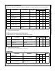
AC Electrical Characteristics, High-Speed
All typical values are V
CC
=2.775V at T
A
=25°C unless otherw ise specified.
Symbol
Parameter
Conditions
T
A
=-40ºC to +85ºC
Units
Min.
Typ.
Max.
t
SK(Part_Part)
Channel-to-Channel Skew
Across Multiple Parts
(8,9)
V
SW
=0.2 Vdiff
PP
, C
L
=5 pF
40
80
ps
t
SK(Chl_Chl)
Channel-to-Channel Skew Within
a Single Part
(8)
V
SW
=0.2 Vdiff
PP
, C
L
=5 pF,
Figure 9
15
30
ps
t
SK(Pulse)
Skew of Opposite Transitions in
the Same Differential Channel
(8)
V
SW
=0.2 Vdiff
PP
, C
L
=5 pF
10
20
ps
Notes:
8. Guaranteed by characterization.
9. Assumes the same V
CC
and temperature for all devices.
Capacitance
Symbol
Parameter
Conditions
T
A
=-40ºC to +85ºC
Units
Min.
Typ.
Max.
C
IN
Control Pin Input
Capacitance
(10)
V
CC
=0 V
1.5
pF
C
ON
Dn/CLK- On Capacitance
(10)
V
CC
=2.775 V, /OE=0 V, f=1 MHz,
at 25°C, Figure 11
6.0
7.0
9.0
C
OFF
Dn/CLK Off Capacitance
(10)
V
CC
=2.775 V
,
/OE=2.775 V,
f=1 MHz, Figure 10
2.5
Note:
10. Guaranteed by characterization.