
Data Sheet

www.onsemi.com
5
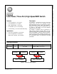
FSA642 — Low-Power, Three-Port, High-Speed MIPI Switch
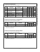
DC Electrical Characteristics
All typical values are T
A
=25°C unless otherw ise specified.
Symbol
Parameter
Conditions
V
CC
(V)
T
A
=-40 to +85ºC
Units
Min.
Typ.
Max.
V
IK
Clamp Diode Voltage
I
IN
=-18 mA
2.775
-1.2
V
I
IN
Control Input Leakage
V
SW
=0 to 4.3 V
4.3
-1
1
µA
V
IH
Input Voltage High
V
IN
=0 to V
CC
2.650 to 2.775
1.3
V
4.3
1.7
V
IL
Input Voltage Low
V
IN
=0 to V
CC
2.650 to 2.775
0.5
V
I
OZ
Off-State Leakage
A,B=0+0.3 V to V
CC
-0.3
4.3
-2
2
µA
I
CC
Quiescent Supply Current
V
CNTRL
=0 or V
CC
, I
OUT
=0
4.3
1.0
µA
I
CCT
Increase in I
CC
Current Per
Control Voltage and V
CC
V
CNTRL
=1.8 V
2.775
1.5
µA
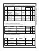
DC Electrical Characteristics, Low-Speed Mode
All typical values are T
A
=25°C unless otherw ise specified.
Symbol
Parameter
Conditions
V
CC
(V)
T
A
=-40 to +85ºC
Units
Min.
Typ.
Max.
R
ON
LS Sw itch On Resistance
(3)
V
SW
=1.2 V, I
ON
=-10 mA, Figure 4
2.65
10
14
∆R
ON
LS Delta R
ON
(4)
V
SW
=1.2 V, I
ON
=-10 mA (Intra-pair)
2.65
0.65
Notes:
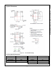
3. Measured by the voltage drop betw een A/B and CLK/Dn pins at the indicated current through the sw itch.
4. Guaranteed by characterization.
DC Electrical Characteristics, High-Speed Mode
All typical values are T
A
=25°C unless otherw ise specified.
Symbol
Parameter
Conditions
V
CC
(V)
T
A
=-40 to +85ºC
Units
Min.
Typ.
Max.
R
ON
HS Sw itch On Resistance
(5)
V
SW
=0.4 V, I
ON
=-10 mA, Figure 4
2.65
7.0
9.5
∆R
ON
HS Delta R
ON
(6)
V
SW
=0.4 V, I
ON
=-10 mA (Intra-pair)
2.65
0.65
Notes:
5. Measured by the voltage drop betw een A, B, and Dn pins at the indicated current through the sw itch.
6. Guaranteed by characterization.