
Data Sheet

www.onsemi.com
4
FSA642 — Low-Power, Three-Port, High-Speed MIPI Switch
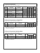
Absolute Maximum Ratings
Stresses exceeding the absolute maximum ratings may damage the device. The device may not function or be
operable above the recommended operating conditions and stressing the parts to these levels is not recommended.
In addition, extended exposure to stresses above the recommended operating conditions may affect device reliability.
The absolute maximum ratings are stress ratings only.
Symbol
Parameter
Min.
Max.
Unit
V
CC
Supply Voltage
-0.50
+5.25
V
V
CNTRL
DC Input Voltage (SEL, /OE)
(1)
-0.5
V
CC
V
V
SW
DC Sw itch I/O Voltage
(1)
-0.5
V
CC
+ 0.3
V
I
IK
DC Input Diode Current
-50
mA
I
OUT
DC Output Current
50
mA
T
STG
Storage Temperature
-65
+150
°C
ESD
Human Body Model, JEDEC: JESD22-A114
All Pins
6.5
kV
I/O to GND
8.0
Pow er to GND
16.0
Charged Device Model, JEDEC: JESD22-C101
2.5
Note:
1. The input and output negative ratings may be exceeded if the input and output diode current ratings are observed.
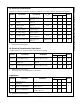
Recommended Operating Conditions
The Recommended Operating Conditions table defines the conditions for actual device operation. Recommended
operating conditions are specified to ensure optimal performance to the datasheet specifications. ON Semiconductor
does not recommend exceeding them or designing to Absolute Maximum Ratings.
Symbol
Parameter
Min.
Max.
Unit
V
CC
Supply Voltage
2.65
4.30
V
V
CNTRL
Control Input Voltage (SEL, /OE)
(2)
0
V
CC
V
V
SW
Sw itch I/O Voltage
-0.5
V
CC
-1
V
T
A
Operating Temperature
-40
+85
°C
Note:
2. The control input must be held HIGH or LOW; it must not float.