
Data Sheet

www.onsemi.com
2
FSA642 — Low-Power, Three-Port, High-Speed MIPI Switch
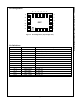
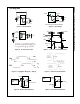
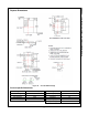
Pin Configuration
D2N
CLKP
CLKN
D1P
D1N
D2P
NC
DB1P
DB1N
CLKBP
CLKBN
DB2P
NC
DA2N
SEL
VCC
GND
/OE
DB2N
CLKAP
CLKAN
DA1P
DA1N
DA2P
642
1 2 3 4 5 6
18 17 16 15 14 13
12
11
10
9
8
7
19
20
21
22
23
24
Figure 2. Pin Configuration (Top Through View)
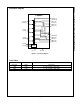
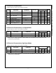
Pin Definitions
Pin #
Name
Description
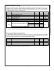
1, 2
CLKP, CLKN
Clock Path (Common)
3, 4
D1P, D1N
Data Path 1 (Common)
5, 6
D2P, D2N
Data Path 2 (Common)
7, 24
NC
No Connect (Float)
8
/OE
Output Enable (Active Low )
9
GND
Ground
10
VCC
Pow er
11
SEL
Select (0=A, 1=B)
12, 13
DA2N, DA2P
Data Path (A2)
14, 15
DA1N, DA1P
Data Path (A1)
16, 17
CLKAN, CLKAP
Clock Path (A)
18, 19
DB2N, DB2P
Data Path (2B)
20, 21
DB1P, DB1N
Data Path (1B)
22, 23
CLKBP, CLKBN,
Clock Path (B)