
Data Sheet

© 2006 Fairchild Semiconductor Corporation www.fairchildsemi.com
FSA2367 • Rev. 1.0.2 8
FSA2367 Low R
ON
(0.75) Triple-SPDT, Negative-Swing Audio Source Switch
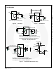
Test Diagrams
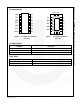
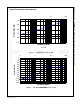
NC
A
I
nA(OFF)
V
IN
GND
V
S1, S2, or S3
= 0 or V
CC
**Each switch port is tested separately
I
nA(OFF)
1B
n,
2B
n,
or 3B
n
1A, 2A, or 3A
I
ON
V
ON
R
ON
= V
ON
/ I
ON
GND
V
IN
GND
V
S1, S2, or S3
= 0 or V
CC
Figure 8. Off Leakage
Figure 9. On Resistance
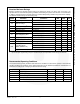
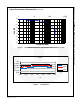
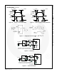
R
L
and C
L
are functions of the application
environment (see AC Tables for specific values)
C
L
includes test fixture and stray capacitance
R
L
C
L
1Bn, 2Bn, or 3Bn
1A, 2A, or 3A
GND
V
IN
GND
V
OUT
S1, S2, S3
L
Figure 10. AC Test Circuit Load
0.9*
V
CC
/2
t
BBM
0V
V
OUT
Input- V
Sel
0.9*
t
RISE
= 2.5ns
90%
10%
C
L
1B0, 2B0, or 3B0
R
L
1A, 2A, or 3A
GND
V
IN1
GND
V
OUT
V
IN2
GND
R
L
and C
L
are functions of the application
environment (see AC Tables for specific values)
C
L
includes test fixture and stray capacitance
S1, S2, S3
--
V
OUT
V
OUT
V
CC
Figure 11. Break-Before-Make Interval Timing