
Data Sheet

© 2006 Fairchild Semiconductor Corporation www.fairchildsemi.com
FSA2367 • Rev. 1.0.2 5
FSA2367 Low R
ON
(0.75) Triple-SPDT, Negative-Swing Audio Source Switch
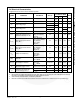
AC Electrical Characteristics
All typical values are for V
CC
=3.3V at 25°C unless otherwise specified.
Symbol
Parameter
Conditions
Vcc (V)
T
A
=- 40ºC to +85ºC
Unit
Min.
Typ.
Max.
t
ON
Turn-On Time, S to Output
V
Bn
=1.5V, R
L
=50Ω,
C
L
=35pF
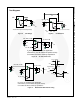
Figure 10, Figure 12
2.7 to 4.3
45
60
ns
t
OFF
Turn-Off Time, S to Output
V
Bn
=1.5V, R
L
=50Ω,
C
L
=35pF
Figure 10, Figure 12
2.7 to 4.3
25
45
ns
t
PD
Propagation Delay
(5)
R
L
=50Ω, C
L
=5pF
Figure 10, Figure 13
3.3
0.25
ns
t
BBM
Break-Before-Make
(5)
R
L
=50Ω, C
L
=35pF
V
IN1=
V
IN2=
V
IN3=
1.5V
Figure 11
2.7 to 4.3
1
6
ns
Q
Charge Injection
R
GEN=
0Ω, C
L
=100pF,
R
L
=OPEN; V
GEN=
0V
Figure 14
2.7 to 4.3
9
pC
O
IRR
Off-Isolation
f=100 kHz, R
L
=50Ω
Figure 4, Figure 16
2.7 to 4.3
-70
dB
Xtalk
Non-Adjacent Channel
Crosstalk
f=100 kHz, R
L
=50Ω
Figure 5, Figure 17
2.7 to 4.3
-100
dB
THD
Total Harmonic Distortion
R
L
=600Ω, V
SW=
0.5V
pp
, f=20
Hz to 20kHz
Figure 20
2.7 to 4.3
0.01
%
BW
-3db bandwidth
R
L
=50Ω, C
L
=0, 5pF
Figure 6, Figure 15
2.7 to 4.3
150
MHz
Note:
5. Guaranteed by characterization; not tested in production.
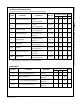
Capacitance
Symbol
Parameter
Conditions
T
A
=- 40ºC to +85ºC
Unit
Min.
Typ.
Max.
C
IN
Control Pin Input Capacitance
V
CC
=0V
2.5
pF
C
ON
A/B On Capacitance
V
CC
=3.3, f=1MHz
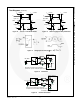
Figure 19
55
C
OFFB
Port 1Bn, 2Bn,3Bn Off Capacitance
V
CC
=3.3, f=1MHz
Figure 18
16
C
OFFA
Port 1A, 2A,3A Off Capacitance
V
CC
=3.3, f=1MHz
Figure 18
20