
Data Sheet

© 2006 Fairchild Semiconductor Corporation www.fairchildsemi.com
FSA2367 • Rev. 1.0.2 4
FSA2367 Low R
ON
(0.75) Triple-SPDT, Negative-Swing Audio Source Switch
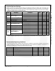
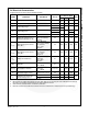
DC Electrical Characteristics
All typical values are at 25°C unless otherwise specified.
Symbol
Parameter
Conditions
Vcc (V)
T
A
=- 40ºC to +85ºC
Unit
Min.
Typ.
Max.
Analog Signal Range
Vcc-
5.5
Vcc
V
V
IK
Clamp Diode Voltage
I
IN
=-18mA
3.0
-1.2
V
V
IH
Input Voltage High
2.7 to 3.6
1.2
V
3.6 to 4.3
1.5
V
IL
Input Voltage Low
2.7 to 3.6
0.5
V
3.6 to 4.3
0.7
I
IN
Control Input Leakage
V
IN
=0 to V
cc
4.3
±1
µA
I
OFF
Power-Off Leakage Current
(Common Port Only 1A, 2A)
Common Port (1A,
2A), V
SW=
0 to 4.3V,
V
CC
=0V
0V
±10
µA
I
NO(0FF)
Off-Leakage Current of Port
1Bn, 2Bn
1Bn, 2Bn=0.5V,
V
CC
- 0.5V or Floating
1A, 2A=0.5V,
V
CC
– 0.5V
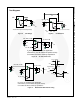
Figure 8
4.3
-250
10
250
nA
I
NC(0N)
On-Leakage Current of Port
1Bn, 2Bn
1Bn, 2Bn=Floating
1A, 2A=0.5V,
V
CC
– 0.5V
Figure 10
4.3
-250
10
250
nA
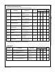
R
ON
Switch On Resistance
(2)
1Bn or 2Bn=0V, 0.7V,
2.0V,2.7V,
I
ON=
-100m
Figure 9
2.7
0.75
2.00
∆R
ON
Delta R
ON
(3)
1Bn or 2Bn=0.7V ,
I
ON=
-100mA
2.7
0.5
R
FLAT(ON)
On Resistance Flatness
(4)
1Bn or 2Bn=0V, 0.7V,
2.0V,2.7V,
I
ON=
-100mA
2.7 to 4.3
0.23
0.40
I
CC
Quiescent Supply Current
V
SW=
0 or V
CC
, I
OUT
=0
4.3
500
nA
I
CCT
Increase in I
CC
Current per
Control Voltage and V
CC
V
CNTRL=
2.6V
4.3
2.2
10.0
µA
V
CNTRL=
1.8V
4.3
6.5
15.0
Notes:
2. Measured by the voltage drop between the 1Bn (2Bn, 3Bn) and 1A (2A, 3A) pins at the indicated current through
the switch. On resistance is determined by the lower voltage on the two.
3. Guaranteed by characterization; not tested in production.
4. Flatness is defined as the difference between minimum and maximum on resistance over the specified range.