
Data Sheet

© 2006 Fairchild Semiconductor Corporation www.fairchildsemi.com
FSA2367 • Rev. 1.0.2 3
FSA2367 Low R
ON
(0.75) Triple-SPDT, Negative-Swing Audio Source Switch
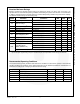
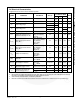
Absolute Maximum Ratings
Stresses exceeding the absolute maximum ratings may damage the device. The device may not function or be
operable above the recommended operating conditions and stressing the parts to these levels is not recommended.
In addition, extended exposure to stresses above the recommended operating conditions may affect device reliability.
The absolute maximum ratings are stress ratings only.
Symbol
Parameter
Conditions
Min.
Max.
Unit
V
CC
Supply Voltages
-0.5
6.0
V
V
SW
Switch I/O Voltage
(1)
1Bn, 2Bn Pins
V
CC
-5.5V
V
CC
-0.3V
V
1A, 2A Pins
V
CC
-5.5V
V
CC
-0.3V
V
V
CNTRL
Control Input Voltage
(1)
S0, S1
-0.5
6.0
V
Input Clamp Diode Current
-50
mA
Switch I/O Current
Continuous
350
mA
Peak Switch Current
Pulsed at 1ms duration, <10% Duty Cycle
500
mA
P
D
Power Dissipation at 85ºC
DQFN14 package
2.5
µW
TSSOP14 package
2.5
µW
T
STG
Storage Temperature Range
-65
+150
C
T
J
Maximum Junction Temperature
+150
C
T
L
Lead Temperature
Soldering, 10 seconds
+260
C
ESD
Human Body Model
(JEDEC: JESD22-A114)
All Pins
5500
kV
I/O to GND
8000
VCC to GND
8000
Charged Device Model (JEDEC-JESD22-C101)
2000
kV
Note:
1. Input and output negative ratings may be exceeded if input and output diode current ratings are observed.
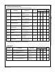
Recommended Operating Conditions
The Recommended Operating Conditions table defines the conditions for actual device operation. Recommended
operating conditions are specified to ensure optimal performance to the datasheet specifications. Fairchild does not
recommend exceeding them or designing to absolute maximum ratings.
Symbol
Parameter
Min.
Max.
Unit
V
CC
Supply Voltages
2.7
4.3
V
V
S0:S1
Control Input Voltage
0
V
CC
V
V
SW
Switch I/O Voltage
V
CC
-5.5
V
CC
-0.3
V
T
A
Operating Temperature
-40
+85
ºC
JA
Thermal Resistance (free air)
145
ºC/W