
Data Sheet


©2009 Fairchild Semiconductor Corporation www.fairchildsemi.com
FODM8061 Rev. 1.1 7
FODM8061 — High Noise Immunity, 3.3V/5V, 10Mbit/sec Logic Gate Output (Open Collector) Optocoupler
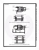
Schematics
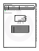
Figure 11. Test Circuit for Propagation Delay Time, Rise Time and Fall Time
Figure 12. Test Circuit for Instantaneous Common Mode Rejection Voltage
Output
350Ω
V
O
Monitoring
Node
t
PHL
C
L
R
M
I
F
0.1μF
Bypass
Pulse Gen.
5MHz
t
f
= tr = 5ns
DC = 50%
Input
Monitoring
Mode
t
f
t
r
t
PLH
(I
F
= 7.5mA)
50%
V
OL
90%
1.5V
10%
Input
350Ω
V
O
(I
F
= 0mA)
V
O
(I
F
= 7.5mA)
V
O
Monitoring
Node
Pulse Gen
V
CC
C
L
V
CM
V
CM
R
M
SW
I
F
0.1μF
Bypass
1kV
0V
V
OH
0.8 V
CC
0.8V
V
OL
90%
10%
t
r
t
f