
Data Sheet

©2009 Fairchild Semiconductor Corporation www.fairchildsemi.com
FODM8061 Rev. 1.1 3
FODM8061 — High Noise Immunity, 3.3V/5V, 10Mbit/sec Logic Gate Output (Open Collector) Optocoupler
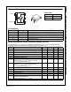
Absolute Maximum Ratings (T
A
=25ºC unless otherwise specified)
Stresses exceeding the absolute maximum ratings may damage the device. The device may not function or be
operable above the recommended operating conditions and stressing the parts to these levels is not recommended. In
addition, extended exposure to stresses above the recommended operating conditions may affect device reliability.
The absolute maximum ratings are stress ratings only.
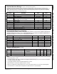
Recommended Operating Conditions
The Recommended Operating Conditions table defines the conditions for actual device operation. Recommended
operating conditions are specified to ensure optimal performance to the datasheet specifications. Fairchild does not
recommend exceeding them or designing to Absolute Maximum Ratings.
Isolation Characteristics (T
A
=25ºC)
Notes:
1. No derate required to 110ºC.
2. Functional operation under these conditions is not implied. Permanent damage may occur if the device is subjected
to conditions outside these ratings.
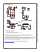
3. 0.1µF bypass capacitor must be connected between pins 4 and 6.
4. Recommended I
FH
is 9.3mA for operation above T
A
=100ºC.
5. Device is considered a two terminal device: Pins 1 and 3 are shorted, and Pins 4, 5, and 6 are shorted together.
6. 3,750 VAC
RMS
for 1 minute duration is equivalent to 4,500 VAC
RMS
for 1 second duration.
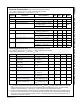
Symbol Parameter Value Units
T
STG
Storage Temperature -40 to +125 ºC
T
OPR
Operating Temperature -40 to +110 ºC
T
J
Junction Temperature -40 to +125 ºC
T
SOL
Lead Solder Temperature
(Refer to Reflow Temperature Profile)
260 for 10sec ºC
I
F
Forward Current 50 mA
V
R
Reverse Voltage 5.0 V
V
CC
Supply Voltage 0 to 7.0 V
V
O
Output Voltage -0.5 to V
CC
+0.5 V
I
O
Average Output Current 50 mA
PD
I
Input Power Dissipation
(1)(2)
100 mW
PD
O
Output Power Dissipation
(1)(2)
85 mW
Symbol Parameter Min. Max. Unit
T
A
Ambient Operating Temperature -40 +110 ºC
V
CC,
V
DD
Supply Voltages
(3)
3.0 5.5 V
V
FL
Logic Low Input Voltage 0 0.8 V
I
FH
Logic High Input Current
(4)
6.3 15 mA
I
FL
Logic Low Input Current 250 µA
N Fan Out (at R
L
= 1kΩ) 5 TTL Loads
R
L
Output Pull-up Resistor 330 4k Ω
Symbol Parameter Test Conditions Min. Typ. Max. Units
V
ISO
Input-Output Isolation Voltage freq= 60Hz, t = 1.0min,
I
I-O
≤ 10µA
(5)(6)
3750
VAC
RMS
R
ISO
Isolation Resistance V
I-O
= 500V
(5)
10
12
Ω
C
ISO
Isolation Capacitance V
I-O
= 0V, freq=1.0MHz
(5)
0.6 pF