
Data Sheet


©2006 Fairchild Semiconductor Corporation www.fairchildsemi.com
FODM30XX Rev. 1.2 4
FODM30XX — 4-Pin Full Pitch Mini-Flat Package Zero-Cross Triac Driver Output Optocouplers
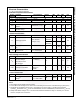
Electrical Characteristics
T
A
= 25°C unless otherwise specified.
Individual Component Characteristics
Transfer Characteristics
Zero Crossing Characteristics
Isolation Characteristics
Notes:
2. Test voltage must be applied within dv/dt rating.
3. This is static dv/dt. See Figure 10 for test circuit. Commutating dv/dt is function of the load-driving thyristor(s) only.
4. All devices are guaranteed to trigger at an I
F
value less than or equal to max I
FT
. Therefore, recommended
operating I
F
lies between max I
FT
(10mA for FODM3062/82, 5mA for FODM3063/83) and absolute max I
F
(60 mA).
5. Steady state isolation voltage, V
ISO
, is an internal device dielectric breakdown rating. For this test, pins 1 & 2 are
common, and pins 3 & 4 are common.
Symbol Parameter Test Conditions Device Min. Typ. Max. Unit
EMITTER
V
F
Input Forward Voltage I
F
= 30 mA All 1.50 V
I
R
Reverse Leakage Current V
R
= 6 V All 100 μA
DETECTOR
I
DRM
Peak Blocking Current Either
Direction
Rated V
DRM
, I
F
= 0
(2)
All 500 nA
dv/dt
Critical Rate of Rise of
Off-State Voltage
I
F
= 0 (Figure 10)
(3)
All 600 V/μs
Symbol Parameter Test Conditions Device Min. Typ. Max. Unit
I
FT
LED Trigger Current
Main Terminal
Voltage = 3 V
(4)
FODM3062,
FODM3082
10
mA
FODM3063,
FODM3083
5
I
H
Holding Current, Either Direc-
tion
All 300 µA
V
TM
Peak On-State Voltage,
Either Direction
I
F
= Rated I
FT
,
I
TM
= 100 mA peak
All 3 V
Symbol Parameter Test Conditions Device Min. Typ. Max. Unit
V
IH
Inhibit Voltage,
MT1-MT2 Voltage
above which device
will not trigger
I
FT
= Rated I
FT
All 20 V
I
DRM2
Leakage in Inhibit State
I
FT
= Rated I
FT
,
Rated V
DRM
,
Off-State
All 2 mA
Symbol Parameter Test Conditions Device Min. Typ. Max. Unit
V
ISO
Steady State Isolation
Voltage
(5)
1 Minute,
R.H. = 40% to 60%
All 3,750 VAC
RMS