
Data Sheet


©2006 Fairchild Semiconductor Corporation www.fairchildsemi.com
FOD852 Rev. 1.5 3
FOD852 — 4-Pin DIP Photodarlington Output Optocoupler
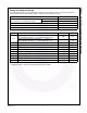
Absolute Maximum Ratings
Stresses exceeding the absolute maximum ratings may damage the device. The device may not function or be
operable above the recommended operating conditions and stressing the parts to these levels is not recommended.
In addition, extended exposure to stresses above the recommended operating conditions may affect device reliability.
The absolute maximum ratings are stress ratings only.
T
A
= 25°C Unless otherwise specified.
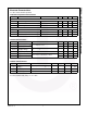
Symbol Parameter Value Units
Total Device
T
STG
Storage Temperature -55 to +125 °C
T
OPR
Operating Temperature -30 to +100 °C
T
J
Junction Temperature -55 to +100 °C
T
SOL
Lead Solder Temperature 260 for 10 seconds °C
P
TOT
Total Device Power Dissipation 200 mW
Input
I
F
Continuous Forward Current 50 mA
V
R
Reverse Voltage 6 V
P
D
LED Power Dissipation 70 mW
Output
V
CEO
Collector-Emitter Voltage 300 V
V
ECO
Emitter-Collector Voltage 0.1 V
I
C
Continuous Collector Current 150 mA
P
C
Collector Power Dissipation 150 mW