
Data Sheet


FNC42060F / FNC42060F2 Motion SPM® 45 Series
©2013 Fairchild Semiconductor Corporation 4 www.fairchildsemi.com
FNC42060F / FNC42060F2 Rev. C3
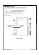
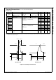
Internal Equivalent Circuit and Input/Output Pins
Figure 3. Internal Block Diagram
1st Notes:
1. Inverter high-side is composed of three IGBTs, freewheeling diodes, and one control IC for each IGBT.
2. Inverter low-side is composed of three IGBTs, freewheeling diodes, and one control IC for each IGBT. It has gate drive and protection functions.
3. Inverter power side is composed of four inverter DC-link input terminals and three inverter output terminals.
COM
VCC
IN(WL)
IN(VL)
IN(UL)
VFO
C(SC)
OUT(WL)
OUT(VL)
OUT(UL)
N
W
(9)
N
V
(8)
N
U
(7)
W(6)
V (5)
U(4)
P (3)
(25) V
S(U)
(26) V
B(U)
(23) V
S(V)
(24) V
B(V)
(10) C
SC
(11) V
FO
(12) IN
(WL)
(13) IN
(VL)
(14) IN
(UL)
(15) COM
UVB
OUT(UH)
UVS
IN(UH)
WVS
WVS
OUT(WH)
IN(WH)
COM
VCC
WVB
OUT(VH)
VVS
IN(VH)
V
TH
(1)
(19) IN
(VH)
(20) IN
(UH)
(21) V
S(W)
(22) V
B(W)
(17) V
CC(H)
(18) IN
(WH)
R
TH
(2)
Thermister
UVS
VVS
VVB
(16) V
CC(L)