
Data Sheet

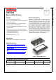
FNB41060 Motion SPM® 45 Series
©2011 Fairchild Semiconductor Corporation 6 www.fairchildsemi.com
FNB41060 Rev. C3
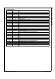
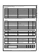
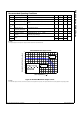
Electrical Characteristics (T
J
= 25°C, unless otherwise specified.)
Inverter Part
2nd Notes:
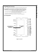
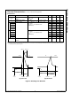
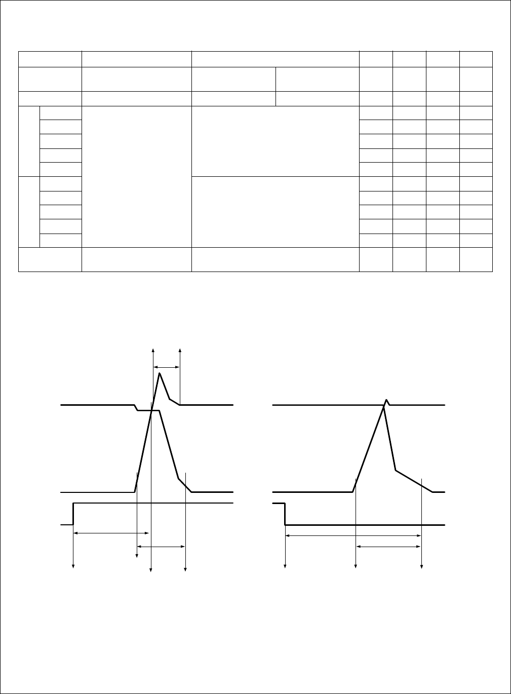
4. t
ON
and t
OFF
include the propagation delay of the internal drive IC. t
C(ON)
and t
C(OFF)
are the switching time of IGBT itself under the given gate driving condition internally. For
the detailed information, please see Figure 4.
Figure 4. Switching Time Definition
Symbol Parameter Conditions Min. Typ. Max. Unit
V
CE(SAT)
Collector - Emitter Saturation
Voltage
V
CC
= V
BS
= 15 V
V
IN
= 5 V
I
C
= 5 A, T
J
= 25°C - 1.5 2.0 V
V
F
FWDi Forward Voltage V
IN
= 0 V I
F
= 5 A, T
J
= 25°C - 1.5 2.0 V
HS t
ON
Switching Times V
PN
= 300 V, V
CC
= V
BS
= 15 V, I
C
= 5 A
T
J
= 25°C
V
IN
= 0 V 5 V, Inductive Load
(2nd Note 4)
0.45 0.75 1.25 s
t
C(ON)
-0.200.45s
t
OFF
-0.701.20s
t
C(OFF)
-0.150.40s
t
rr
-0.15- s
LS t
ON
V
PN
= 300 V, V
CC
= V
BS
= 15 V, I
C
= 5 A
T
J
= 25°C
V
IN
= 0 V 5 V, Inductive Load
(2nd Note 4)
0.35 0.65 1.15 s
t
C(ON)
-0.150.40s
t
OFF
-0.651.15s
t
C(OFF)
-0.150.40s
t
rr
-0.15- s
I
CES
Collector - Emitter Leakage
Current
V
CE
= V
CES
--1mA
V
CE
I
C
V
IN
t
ON
t
C(ON)
V
IN(ON)
10% I
C
10% V
CE
90% I
C
100% I
C
t
rr
100% I
C
V
CE
I
C
V
IN
t
OFF
t
C(OFF)
V
IN(OFF)
10% V
CE
10% I
C
(a) turn-on
(b) turn-off