
Data Sheet
FNB41060 Motion SPM® 45 Series
©2011 Fairchild Semiconductor Corporation 9 www.fairchildsemi.com
FNB41060 Rev. C3
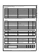
Recommended Operating Conditions
2nd Notes:
8. This product might not make response if input pulse width is less than the recommanded value.
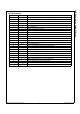
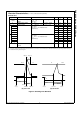
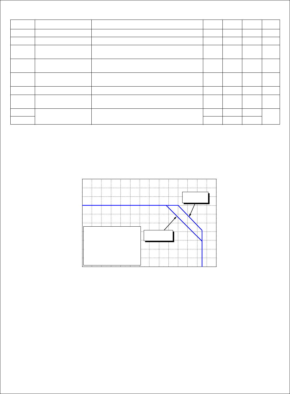
Figure 8. Allowable Maximum Output Current
2nd Notes:
9. This allowable output current value is the reference data for the safe operation of this product. This may be different from the actual application and operating condition.
Symbol Parameter Conditions Min. Typ. Max. Unit
V
PN
Supply Voltage Applied between P - N
U
, N
V
, N
W
- 300 400 V
V
CC
Control Supply Voltage Applied between V
CC(H)
, V
CC(L)
- COM 13.5 15 16.5 V
V
BS
High-Side Bias Voltage Applied between V
B(U)
- V
S(U)
, V
B(V)
- V
S(V)
, V
B(W)
-
V
S(W)
13.0 15 18.5 V
dV
CC
/ dt,
dV
BS
/ dt
Control Supply Variation - 1 - 1 V /
s
t
dead
Blanking Time for
Preventing Arm-Short
For each input signal 1.5 - - s
f
PWM
PWM Input Signal - 40C <T
J
<150°C - - 20 kHz
V
SEN
Voltage for Current
Sensing
Applied between N
U
, N
V
, N
W
- COM
(Including Surge-Voltage)
- 4 4 V
P
WIN(ON)
Minimun Input Pulse
Width
(2nd Note 8) 0.5 - - s
P
WIN(OFF)
0.5 - -
0 102030405060708090100110120130140
0
1
2
3
4
5
6
7
8
9
10
Allowable Maximum Output Current
V
DC
=300V, V
CC
=V
BS
=15V
T
J
< 150℃ , T
C
≤ 125℃
M.I.=0.9, P.F.=0.8
Sinusoidal PWM
f
SW
=15kHz
f
SW
=5kHz
Allowable Output Current, I
Orms
[A
rms
]
Case Temperature, T
C
[℃]