
Data Sheet


© 2008 Fairchild Semiconductor Corporation www.fairchildsemi.com
FMS6363A • Rev. 2.0.2 4
FMS6363A —Three-Channel 7
th
-Order High-Definition VoltagePlus™ Video Filter Driver
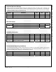
DC Electrical Characteristics
Unless otherwise noted
T
A
=25°C, V
CC
=3.3V, R
S
=37.5; all inputs are AC-coupled with 0.1µF; all output AC-coupled
with 220µF into 150 load.
Symbol Parameter Conditions Min. Typ. Max. Units
Supply
V
S
Supply Voltage Range V
S
Range 3.14 3.30 5.25 V
I
CC
Quiescent Supply Current
(1)
V
S
=+3.3V, No Load 22 35 mA
V
S
=+5V, No Load 34 40 mA
V
IN
Video Input Voltage Range
Referenced to GND if
DC Coupled
1.4 V
PP
PSRR Power Supply Rejection Ratio DC (All Channels) -60 dB
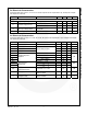
AC Electrical Characteristics
Unless otherwise noted, T
A
=25°C, V
CC
=3.3V, R
S
=37.5; all inputs are AC-coupled with 0.1µF; all outputs AC-coupled
with 220µF into 150 load.
Symbol Parameter Conditions Min. Typ. Max. Units
AV Channel Gain Active Video Input Range = 1V
PP
5.8 6.0 6.2 dB
BW
0.5dB
±0.5dB Bandwidth
R
SOURCE
=75, R
L
=150
28 MHz
BW
-1.0dB
-1.0 dB Bandwidth 26 30 MHz
BW
3.0dB
-3.0 dB Bandwidth 30 34 MHz
Att
37.125M
Normalized Stopband
Attenuation
R
SOURCE
=75, f=37.325MHz 6.5
dB
Att
44.25M
R
SOURCE
=75, f=44.25MHz 14.5
Att
74.25M
R
SOURCE
=75, f=74.25MHz 40 44
Att
78M
R
SOURCE
=75, f=78MHz 46
THD1
Output Distortion
(All Channels)
f=10 MHz; V
OUT
=1.4V
PP
-49
dBC
THD2 f=15 MHz; V
OUT
=1.4V
PP
-48
THD3 f=22 MHz; V
OUT
=1.4V
PP
-45
X
talk
Crosstalk
(Channel-to-Channel)
f=1.00 MHz; V
OUT
=1.4V
PP
-65 dB
SNR Peak Signal to RMS Noise
Unweighted: 30MHz Lowpass,
100kHz to 30MHz
65 dB
t
pd
Propagation Delay
Delay from Input to Output;
100KHz to 28MHz
12 ns