
Data Sheet


© 2008 Fairchild Semiconductor Corporation www.fairchildsemi.com
FMS6363A • Rev. 2.0.2 3
FMS6363A —Three-Channel 7
th
-Order High-Definition VoltagePlus™ Video Filter Driver
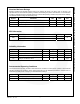
Absolute Maximum Ratings
Stresses exceeding the absolute maximum ratings may damage the device. The device may not function or be
operable above the recommended operating conditions and stressing the parts to these levels is not recommended.
In addition, extended exposure to stresses above the recommended operating conditions may affect device reliability.
The absolute maximum ratings are stress ratings only.
Symbol Parameter Min. Max. Unit
V
S
DC Supply Voltage -0.3 6.0 V
V
IO
Analog and Digital I/O -0.3 V
CC
+0.3 V
V
OUT
Maximum Output Current, Do Not Exceed 50 mA
ESD Information
Symbol Parameter Min Unit
ESD
Human Body Model, JESD22-A114 9
kV
Charged Device Model, JESD22-C101 2
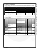
Reliability Information
Symbol Parameter Min. Typ. Max. Unit
T
J
Junction Temperature +150 °C
T
STG
Storage Temperature Range -65 +150 °C
T
L
Lead Temperature (Soldering, 10s) +300 °C
JA
Thermal Resistance, JEDEC Standard,
Multilayer Test Boards, Still Air
115 °C/W
Recommended Operating Conditions
The Recommended Operating Conditions table defines the conditions for actual device operation. Recommended
operating conditions are specified to ensure optimal performance to the datasheet specifications. Fairchild does not
recommend exceeding them or designing to Absolute Maximum Ratings.
Symbol Parameter Min. Typ. Max. Unit
T
A
Operating Temperature Range -40 +85 °C
V
CC
Supply Voltage Range 3.14 3.30 5.25 V