
Data Sheet


© 2008 Fairchild Semiconductor Corporation www.fairchildsemi.com
FMS6363A • Rev. 2.0.2 2
FMS6363A —Three-Channel 7
th
-Order High-Definition VoltagePlus™ Video Filter Driver
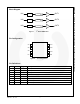
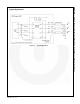
Block Diagram
IN1
IN2
IN3
OUT1
OUT2
OUT3
6d
B
Clamp
6d
B
Bias
6d
B
Bias
Figure 1. 7
th
-Order 30MHz Filter
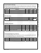
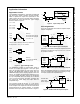
Pin Configuration
IN1
OUT1
IN2
IN3
OUT
3
V
CC
OUT
2
GND
1
2
3
4
8
7
6
5
Figure 2. Pin Configuration
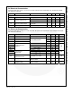
Pin Definitions
Pin# Name Type Description
1 IN1 Input Video Input Channel 1
2 IN2 Input Video Input Channel 2
3 IN3 Input Video Input Channel 2
4 V
CC
Input Positive Power Supply
5 GND Input Device Ground Connection
6 OUT3 Output Filtered Output Channel 3
7 OUT2 Output Filtered Output Channel 2
8 OUT1 Output Filtered Output Channel 1