
Data Sheet


© 2011 Fairchild Semiconductor Corporation www.fairchildsemi.com
FDMF6705B • Rev. 1.0.3 16
FDMF6705B - Extra-Small, High-Performance, High-Frequency DrMOS Module
PCB Layout Guidelines
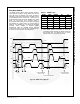
Figure 30 provides an example of a proper layout for
critical components. All of the high-current paths, such
as V
IN
, V
SWH
, V
OUT
, and GND copper, should be short
and wide for low inductance and resistance. This
technique achieves a more stable and evenly distributed
current flow, along with enhanced heat radiation and
system performance.
The following guidelines are recommendations for the
PCB designer:
1. Input ceramic bypass capacitors must be placed
close to the VIN and PGND pins. This helps reduce
the high-current power loop inductance and the input
current ripple induced by the power MOSFET
switching operation.
2. The V
SWH
copper trace serves two purposes. In
addition to being the high-frequency current path
from the DrMOS package to the output inductor, it
also serves as a heat sink for the low-side MOSFET
in the DrMOS package. The trace should be short
and wide enough to present a low-impedance path
for the high-frequency, high-current flow between the
DrMOS and inductor to minimize losses and
temperature rise. Note that the VSWH node is a
high-voltage and high-frequency switching node with
high noise potential. Care should be taken to
minimize coupling to adjacent traces. Since this
copper trace also acts as a heat sink for the lower
FET, balance using the largest area possible to
improve DrMOS cooling while maintaining
acceptable noise emission.
3. An output inductor should be located close to the
FDMF6705B to minimize the power loss due to the
VSWH copper trace. Care should also be taken so
the inductor dissipation does not heat the DrMOS.
4. PowerTrench
®
MOSFETs are used in the output
stage. The power MOSFETs are effective at
minimizing ringing due to fast switching. In most
cases, no VSWH snubber is required. If a snubber is
used, it should be placed close to the VSWH and
PGND pins. The resistor and capacitor need to be of
proper size for the power dissipation.
5. VCIN, VDRV, and BOOT capacitors should be
placed as close as possible to the VCIN to CGND,
VDRV to CGND, and BOOT to PHASE pins to
ensure clean and stable power. Routing width and
length should be considered.
6. Include a trace from PHASE to VSWH to improve
noise margin. Keep the trace as short as possible.
7. The layout should include a place holder to insert a
small-value series boot resistor (R
BOOT
) between the
boot capacitor (C
BOOT
) and DrMOS BOOT pin. The
BOOT-to-VSWH loop size, including R
BOOT
and
C
BOOT
, should be as small as possible. The boot
resistor may be required when operating near the
maximum rated V
IN
. The boot resistor is effective at
controlling the high-side MOSFET turn-on slew rate
and VSHW overshoot. R
BOOT
can improve noise
operating margin in synchronous buck designs that
have noise issues due to ground bounce or high
positive and negative VSWH ringing. However,
inserting a boot resistance lowers the DrMOS
efficiency. Efficiency versus noise trade-offs must be
considered. R
BOOT
values from 0.5 to 3.0 Ω are
typically effective in reducing VSWH overshoot.
The VIN and PGND pins handle large current
transients with frequency components greater than
100 MHz. If possible, these pins should be
connected directly to the VIN and board GND
planes. The use of thermal relief traces in series with
these pins is discouraged
since this adds
inductance to the power path. This added inductance
in series with either the VIN or PGND pin degrades
system noise immunity by increasing positive and
negative VSWH ringing.
8. CGND pad and PGND pins should be connected to
the GND plane copper with multiple vias for stable
grounding. Poor grounding can create a noise
transient offset voltage level between CGND and
PGND. This could lead to faulty operation of the
gate driver and MOSFETs.
9. Ringing at the BOOT pin is most effectively
controlled by close placement of the boot capacitor.
Do not add an additional BOOT to the PGND
capacitor. This may lead to excess current flow
through the BOOT diode.
10. The SMOD# and DISB# pins have weak internal
pull-up and pull-down current sources, respectively.
These pins should not have any noise filter
capacitors. Do not to float these pins unless
absolutely necessary.
11. Use multiple vias on each copper area to
interconnect top, inner, and bottom layers to help
distribute current flow and heat conduction. Vias
should be relatively large and of reasonably low
inductance. Critical high-frequency components,
such as R
BOOT
, C
BOOT
, the RC snubber, and bypass
capacitors should be located as close to the
respective DrMOS module pins as possible on the
top layer of the PCB. If this is not feasible, they
should be connected from the backside through a
network of low-inductance vias.