
Data Sheet


© 2011 Fairchild Semiconductor Corporation www.fairchildsemi.com
FDMF6705B • Rev. 1.0.3 15
FDMF6705B - Extra-Small, High-Performance, High-Frequency DrMOS Module
Application Information
Supply Capacitor Selection
For the supply inputs (VDRV and VCIN), a local ceramic
bypass capacitor is required to reduce noise and to
supply peak transient currents during gate drive
switching action. It is recommended to use a minimum
capacitor value of 1 µF X7R or X5R. Keep this capacitor
close to the VCIN and VDRV pins and connect it to the
GND plane with vias.
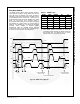
Bootstrap Circuit
The bootstrap circuit uses a charge storage capacitor
(C
BOOT
), as shown in Figure 28. A bootstrap capacitance
of 100 nF X7R or X5R capacitor is typically adequate. A
series bootstrap resistor may be needed for specific
applications to improve switching noise immunity. The
boot resistor (R
BOOT
) may be required when operating
near the maximum rated V
IN
and is effective at
controlling the high-side MOSFET turn-on slew rate and
VSHW overshoot. Typical R
BOOT
values from 0.5 to
3.0 Ω are effective in reducing VSWH overshoot.
VCIN Filter
The VDRV pin provides power to the gate drive of the
high-side and low-side power MOSFETs. In most cases,
VDRV can be connected directly to VCIN, which
supplies power to the logic circuitry of the gate driver.
For additional noise immunity, an RC filter can be
inserted between VDRV and VCIN. Recommended
values of 10 Ω (R
VCIN
) placed between VDRV and VCIN
and 1 µF (C
VCIN
) from VCIN to CGND, Figure 28.
Power Loss and Efficiency
Measurement and Calculation
Refer to Figure 29 for power-loss testing method. Power
loss calculations are:
P
IN
=(V
IN
x I
IN
) + (V
5V
x I
5V
) (W)
(1)
P
SW
=V
SW
x I
OUT
(W)
(2)
P
OUT
=V
OUT
x I
OUT
(W)
(3)
P
LOSS_MODULE
=P
IN
- P
SW
(W)
(4)
P
LOSS_BOARD
=P
IN
- P
OUT
(W)
(5)
EFF
MODULE
=100 x P
SW
/P
IN
(%)
(6)
EFF
BOARD
=100 x P
OUT
/P
IN
(%)
(7)
Figure 28. Block Diagram with V
CIN
Filter
Figure 29. Power Loss Measurement
V
OUT