
Data Sheet


© 2011 Fairchild Semiconductor Corporation www.fairchildsemi.com
FDMF6705B • Rev. 1.0.3 13
FDMF6705B - Extra-Small, High-Performance, High-Frequency DrMOS Module
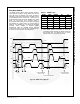
Adaptive Gate Drive Circuit
The driver IC advanced design ensures minimum
MOSFET dead time, while eliminating potential shoot-
through (cross-conduction) currents. It senses the state
of the MOSFETs and adjusts the gate drive adaptively
to ensure they do not conduct simultaneously. Figure 26
provides the relevant timing waveforms. To prevent
overlap during the LOW-to-HIGH switching transition
(Q2 off to Q1 on), the adaptive circuitry monitors the
voltage at the GL pin. When the PWM signal goes
HIGH, Q2 turns off after a propagation delay (t
PD_PHGLL
).
Once the GL pin is discharged below ~1 V, Q1 turns on
after adaptive delay, t
D_DEADON
.
To preclude overlap during the HIGH-to-LOW transition
(Q1 off to Q2 on), the adaptive circuitry monitors the
voltage at the VSWH pin. When the PWM signal goes
LOW, Q1 turns off after a propagation delay (t
PD_PLGHL
).
Once the VSWH pin falls below ~2.2 V, Q2 turns on
after adaptive delay, t
D_DEADOFF
. Additionally, V
GS(Q1)
is
monitored. When V
GS(Q1)
is discharged below ~1.2 V, a
secondary adaptive delay is initiated, which results in
Q2 being driven on after t
D_TIMEOUT
, regardless of SW
state. This function is implemented to ensure C
BOOT
is
recharged each switching cycle in the event that the SW
voltage does not fall below the 2.2 V adaptive threshold.
Secondary delay t
D_TIMEOUT
is longer than t
D_DEADOFF
.
Figure 26. PWM and 3-StateTiming Diagram
Notes:
t
PD_xxx
= propagation delay from external signal (PWM, SMOD#, etc.) to IC generated signal. Example (t
PD_PHGLL
– PWM going HIGH to LS V
GS
(GL) going LOW)
t
D_xxx
= delay from IC generated signal to IC generated signal. Example (t
D_DEADON
– LS V
GS
(GL) LOW to HS V
GS
(GH) HIGH)
PWM Exiting 3-state
t
PD_PHGLL
= PWM rise to LS V
GS
fall, V
IH_PWM
to 90% LS V
GS
t
PD_TSGHH
= PWM 3-state to HIGH to HS V
GS
rise, V
IH_PWM
to 10% HS V
GS
t
PD_PLGHL
= PWM fall to HS V
GS
fall, V
IL_PWM
to 90% HS V
GS
t
PD_TSGLH
= PWM 3-state to LOW to LS V
GS
rise, V
IL_PWM
to 10% LS V
GS
t
PD_PHGHH
= PWM rise to HS V
GS
rise, V
IH_PWM
to 10% HS V
GS
(SMOD# held LOW)
SMOD# Dead Times
t
PD_SLGLL
= SMOD# fall to LS V
GS
fall, V
IL_SMOD
to 90% LS V
GS
t
D_DEADON
= LS V
GS
fall to HS V
GS
rise, LS-comp trip value (~1.0V GL) to 10% HS V
GS
t
PD_SHGLH
= SMOD# rise to LS V
GS
rise, V
IH_SMOD
to 10% LS V
GS
t
D_DEADOFF
= VSWH fall to LS V
GS
rise, SW-comp trip value (~2.2V VSWH) to 10% LS V
GS
t
PD_TSGHH
VSWH
GH
to
VSWH
GL
t
PD_PHGLL
t
D_HOLD -OFF
90%
less than
t
D_HOLD -
OFF
Exit
3 S t a t e
1.0V
PWM
V
IL_PWM
V
IH_PWM
V
TRI_HI
V
IH_PWM
V
IH_PWM
10%
t
R_GL
t
D_HOLD -
OFF
t
PD_TSGLH
less than
t
D_HOLD
-
OFF
Exit
3-State
V
IH PWM
V
TRI_HI
V
TRI_LO
V
IL_PWM
t
PD
_
PLGHL
t
PD_TSGHH
DCM
t
F_GH
t
R_GH
t
D_HOLD
-OFF
10%
CCM
DCM
Exit
3-
State
90%
1
0%
90%
Enter
3
-State
Enter
3 -
State
t
D_DEADOFF
t
D_DEADON
Enter
3
-
State
t
F_GL
V
IN
V
OUT
2.2
V