
Data Sheet


© 2011 Fairchild Semiconductor Corporation www.fairchildsemi.com
FDMF6705B • Rev. 1.0.3 12
FDMF6705B - Extra-Small, High-Performance, High-Frequency DrMOS Module
Functional Description
The FDMF6705B is a driver-plus-FET module optimized
for the synchronous buck converter topology. A single
PWM input signal is all that is required to properly drive
the high-side and the low-side MOSFETs. Each part is
capable of driving speeds up to 1 MHz.
VCIN and Disable
The VCIN pin is monitored by an Under-Voltage Lockout
(UVLO) circuit. When V
CIN
rises above ~3.1 V, the driver
is enabled. When V
CIN
falls below ~2.7 V, the driver is
disabled (GH, GL=0). The driver can also be disabled by
pulling the DISB# pin LOW (DISB# < V
IL_DISB
), which
holds both GL and GH LOW regardless of the PWM
input state. The driver can be enabled by raising the
DISB# pin voltage HIGH (DISB# > V
IH_DISB
).
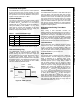
Table 1. UVLO and Disable Logic
UVLO DISB# Driver State
0 X Disabled (GH, GL=0)
1 0 Disabled (GH, GL=0)
1 1 Enabled (See Table 2)
1 Open Disabled (GH, GL=0)
Note:
3. DISB# internal pull-down current source is 10 µA.
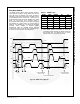
Thermal Warning Flag
The FDMF6705B provides a thermal warning flag
(THWN) to warn of over-temperature conditions. The
thermal warning flag uses an open-drain output that
pulls to CGND when the activation temperature (150°C)
is reached. The THWN output returns to a high-
impedance state once the temperature falls to the reset
temperature (135°C). The THWN output requires a pull-
up resistor, which can be connected to VCIN. THWN
does NOT disable the DrMOS module.
Figure 25. THWN Operation
3-State PWM Input
The FDMF6705B incorporates a three-state PWM input
gate drive design. The three-state gate drive has both
logic HIGH level and LOW level, along with a three-state
shutdown window. When the PWM input signal enters
and remains within the three-state window for a defined
hold-off time (t
D_HOLD-OFF
), both GL and GH are pulled
LOW. This feature enables the gate drive to shut down
both high-and low-side MOSFETs to support features
such as phase shedding, which is a common feature on
multiphase voltage regulators.
Operation when Exiting Three-State
Condition
When exiting a valid three-state condition, the
FDMF6705B design follows the PWM input command. If
the PWM input goes from three-state to LOW, the low-
side MOSFET is turned on. If the PWM input goes from
three-state to HIGH, the high-side MOSFET is turned
on. This is illustrated in Figure 26. The FDMF6705B
design allows for short propagation delays when exiting
the three-state window (see Electrical Characteristics).
Low-Side Driver
The low-side driver (GL) is designed to drive a ground-
referenced low R
DS(ON)
N-channel MOSFET. The bias
for GL is internally connected between VDRV and
CGND. When the driver is enabled, the driver's output is
180° out of phase with the PWM input. When the driver
is disabled (DISB#=0 V), GL is held LOW.
High-Side Driver
The high-side driver is designed to drive a floating N-
channel MOSFET. The bias voltage for the high-side
driver is developed by a bootstrap supply circuit,
consisting of the internal Schottky diode and external
bootstrap capacitor (C
BOOT
). During startup, VSWH is
held at PGND, allowing C
BOOT
to charge to VDRV
through the internal diode. When the PWM input goes
HIGH, GH begins to charge the gate of the high-side
MOSFET (Q1). During this transition, the charge is
removed from C
BOOT
and delivered to the gate of Q1. As
Q1 turns on, V
SWH
rises to V
IN
, forcing the BOOT pin to
V
IN
+ V
BOOT
, which provides sufficient V
GS
enhancement
for Q1. To complete the switching cycle, Q1 is turned off
by pulling GH to VSWH. C
BOOT
is then recharged to
VDRV when VSWH falls to PGND. GH output is in-
phase with the PWM input. The high-side gate is held
LOW when the driver is disabled or the PWM signal is
held within the three-state window for longer than the
three-state hold-off time, t
D_HOLD-OFF
.
150°C
A
ctivation
Tem
p
erature
T
J_driverIC
Thermal
Warning
Normal
Operation
HIGH
LOW
THWN
Logic
State
135°C
Reset