
Data Sheet

© 2008 Fairchild Semiconductor Corporation www.fairchildsemi.com
FAN8303 • Rev. 1.2 3
FAN8303 — 2 A 23 V Non-Synchronous Step-Down DC/DC Regulator
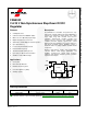
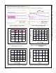
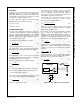
Pin Configuration
Figure 3. Pin Configuration (Top View)
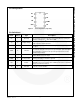
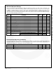
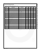
Pin Definitions
Name
Pin #
Type
Description
BS
1
Bootstrap
High-Side Drive BOOT Voltage. Connect through capacitor (C
BS
) to SW.
The IC includes an internal synchronous bootstrap diode to recharge the
capacitor on this pin to V
CC
when SW is LOW.
VIN
2
Supply Voltage
Power Input. This pin needs to be closely decoupled to the GND pin with a
10 µF or greater ceramic capacitor.
SW
3
Switch
Power Switching Output. SW is the switching node that supplies power to
the output.
GND
4
Ground
Power Return and Signal Ground for the IC. All internal control voltages
are referred to this pin. Tie this pin to the ground island / plane through the
lowest impedance connection. This pin is the ground reference for the
regulated output voltage.
FB
5
Feedback
Feedback Input. This pin is the center tap of the external feedback voltage
resistive divider across the output.
COMP
6
Compensation
Compensation Node. Frequency compensation is accomplished at this
node by connecting a series R-C to ground.
EN
7
Enable
Enable Input. EN is a digital input that turns the regulator on or off. Drive
EN HIGH to turn on the regulator, drive it LOW to turn it off. For automatic
startup, leave EN unconnected.
SS
8
Soft Start
External Soft-Start. A capacitor connected between this pin and GND can
be used to set soft-start time.
BS
VIN
SW
GND
FB
COMP
EN
SS