
Data Sheet

© 2008 Fairchild Semiconductor Corporation www.fairchildsemi.com
FAN8303 • Rev. 1.2 10
FAN8303 — 2 A 23 V Non-Synchronous Step-Down DC/DC Regulator
Design example
Assume the V
IN
voltage is 12 V with a 10% tolerance.
The maximum load current is 2 A and the output voltage
is set to 2.5 V at 2 A maximum load. Calculate the
inductor value from the following formula:
MAXIN
OUT
MAXLOSC
OUT
V
V
If
V
L
,,
1
(14)
Substituting V
OUT
=2.5 V, V
IN,MAX
=12 V, Δ I
L,MAX
=0.4 A,
and f
S
= 370 kHz in the formula gives:
H
AkHz
L
13
12
5.2
1
4.0370
5.2
(15)
A 15 µH inductor is chosen for this application.
If the V
OUT
voltage is 2.5 V, choose R2=18kΩ(1%), and
R3 can be calculated from:
kkR 68.5
6.05.2
6.0
183
(16)
Choose R3=5.6 kΩ(1%).
In this application, with the desired crossover frequency
at 30 kHz, R
C
value is calculated as follows:
VVAVA
VkHzF
R
C
6.0/380/2
5.230222
(17)
If R
C
=22.72 kΩ, choose 22 kΩ for the design.
If R
C
=22 kΩ, use the following equation to get C
C
:
kHzk
C
C
3022
2
Ω
(18)
C
C
= 0.965 nF, choose 1 nF for the design.
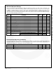
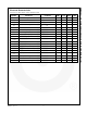
Table 1. Recommended Compensation Values
(V
IN
=12 V)
V
O
L
C
OUT
R
2
R
3
R
C
C
C
1.8 V
10 µH
22 µF
MLCC
18 kΩ
9 kΩ
16 kΩ
1.5 nF
2.5 V
15 µH
5.6 kΩ
22 kΩ
1 nF
3.3 V
15 µH
4 kΩ
27 kΩ
820 pF
5 V
22 µH
2.45 kΩ
43 kΩ
560 pF
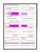
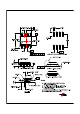
Layout Consideration
As with all switching power supplies, careful attention to
PCB layout is important to the design. A few design
rules should be implemented to ensure good layout:
Keep the high-current traces and load connections
as short as possible.
Place the input capacitor, the inductor, the
freewheeling diode, and the output capacitor as
close as possible to the IC terminals.
Keep the loop area between the SW node,
freewheeling diode, inductor, and output capacitor
as small as possible. Minimizing ground loops
reduces EMI issues.
Route high-dV/dt signals, such as SW node, away
from the error amplifier input/output pins. Keep
components connected to these pins close to the
pins.
To effectively remove heat from the MOSFETs, use
wide land areas with appropriate thermal vias.
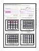
Figure 17. Recommended PCB Layout
The table below pertains to Marketing outline drawing on the following page.
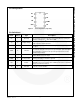
Package Dimensions
Symbol
Millimeter
Inch
Min.
Typ.
Max.
Min.
Typ.
Max.
A
1.346
1.752
0.053
0.069
A1
0.101
0.254
0.004
0.010
b
0.406
0.016
c
0.203
0.008
D
4.648
4.978
0.183
0.196
E
3.810
3.987
0.150
0.157
e
1.270
0.050
F
0.381X45˚
0.015X45˚
H
5.791
6.197
0.228
0.244
L
0.406
1.270
0.016
0.050
θ˚
0˚
8˚
0˚
8˚