
Data Sheet

www.onsemi.com
4
FAN7930C — Critical Conduction Mode PFC Controller
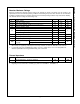
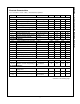
Absolute Maximum Ratings
Stresses exceeding the absolute maximum ratings may damage the device. The device may not function or be
operable above the recommended operating conditions and stressing the parts to these levels is not recommended.
In addition, extended exposure to stresses above the recommended operating conditions may affect device reliability.
The absolute maximum ratings are stress ratings only.
Symbol
Parameter
Min.
Max.
Unit
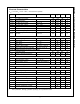
V
CC
Supply Voltage
V
Z
V
I
OH
, I
OL
Peak Drive Output Current
-800
+500
mA
I
CLAMP
Driver Output Clamping Diodes V
O
>V
CC
or V
O
<-0.3 V
-10
+10
mA
I
DET
Detector Clamping Diodes
-10
+10
mA
V
IN
RDY Pin
(
1
)
V
Z
V
Error Amplifier Input, Output and ZCD
(
1
)
-0.3
8.0
CS Input Voltage
(
2
)
-10.0
6.0
T
J
Operating Junction Temperature
+150
°C
T
A
Operating Temperature Range
-40
+125
°C
T
STG
Storage Temperature Range
-65
+150
°C
ESD
Electrostatic Discharge
Capability
Human Body Model, JESD22-A114
2.5
kV
Charged Device Model, JESD22-C101
2.0
Notes:
1. When this pin is supplied by external pow er sources by accident, its maximum allow able current is 50 mA .
2. In case of DC input, the acceptable input range is -0.3 V~6 V: w ithin 100 ns -10 V~6 V is acceptable, but
electrical specifications are not guaranteed during such a short time.
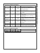
Thermal Impedance
Symbol
Parameter
Min.
Max.
Unit
JA
Thermal Resistance, Junction-to-Ambient
(
3
)
150
°C/W
Note:
3. Regarding the test environment and PCB type, please refer to JESD51-2 and JESD51-10.