
Data Sheet

www.onsemi.com
3
FAN7930C — Critical Conduction Mode PFC Controller
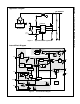
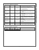
Pin Configuration
INV RDY CS
ZCD
FAN7930C
8-SOP
COMP
V
CC
OUT GND
Figure 3. Pin Configuration (Top View)
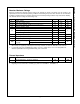
Pin Definitions
Pin #
Name
Description
1
INV
This pin is the inverting input of the error amplifier. The output voltage of the boost PFC converter
should be resistively divided to 2.5 V.
2
RDY
This pin is used to detect PFC output voltage reaching a pre-determined value. When output
voltage reaches 89% of rated output voltage, this pin is pulled HIGH, w hich is an (open-drain)
output type.
3
COMP
This pin is the output of the transconductance error amplifier. Components for the output voltage
compensation should be connected betw een this pin and GND.
4
CS
This pin is the input of the over-current protection comparator. The MOSFET current is sensed
using a sensing resistor and the resulting voltage is applied to this pin. An internal RC filter is
included to filter sw itching noise.
5
ZCD
This pin is the input of the zero-current detection (ZCD) block. If the voltage of this pin goes
higher than 1.5 V, then goes low er than 1.4 V, the MOSFET is turned on.
6
GND
This pin is used for the ground potential of all the pins. For proper operation, the signal ground
and the pow er ground should be separated.
7
OUT
This pin is the gate drive output. The peak sourcing and sinking current levels are +500 mA and
-800 mA , respectively. For proper operation, the stray inductance in the gate driving path must be
minimized.
8
V
CC
This is the IC supply pin. IC current and MOSFET drive current are supplied using this pin.