
Data Sheet

www.onsemi.com
21
FAN7930C — Critical Conduction Mode PFC Controller
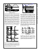
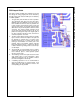
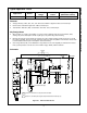
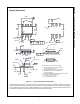
Physical Dimensions
Figure 47. 8-Lead, Small Outline Package (SOP)
Package drawings are provided as a service to customers considering ON Semiconductor components. Drawings may change in
any manner without notice. Please note the revision and/or date on the drawing and contact a ON Semiconductor representative to
verify or obtain the most recent revision. Package specifications do not expand the terms of ON Semiconductor’s worldwide terms
and conditions, specifically the warranty therein, which covers ON Semiconductor products.
8°
0°
SEE DETAIL A
NOTES: UNLESS OTHERWISE SPECIFIED
A) THIS PACKAGE CONFORMS TO JEDEC
MS-012, VARIATION AA.
B) ALL DIMENSIONS ARE IN MILLIMETERS.
C) DIMENSIONS DO NOT INCLUDE MOLD
FLASH OR BURRS.
D) LANDPATTERN STANDARD: SOIC127P600X175-8M.
E) DRAWING FILENAME: M08Arev14
F) FAIRCHILD SEMICONDUCTOR.
LAND PATTERN RECOMMENDATION
SEATING PLANE
C
GAGE PLANE
x 45°
DETAIL A
SCALE: 2:1
PIN ONE
INDICATOR
4
8
1
B
5
A
5.60
0.65
1.75
1.27
6.20
5.80
3.81
4.00
3.80
5.00
4.80
(0.33)
1.27
0.51
0.33
0.25
0.10
1.75 MAX
0.25
0.19
0.36
0.50
0.25
R0.10
R0.10
0.90
0.40
(1.04)
OPTION A - BEVEL EDGE
OPTION B - NO BEVEL EDGE
0.25 C B A
0.10