
Data Sheet

www.onsemi.com
2
FAN7930C — Critical Conduction Mode PFC Controller
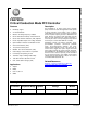
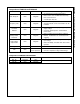
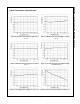
Application Diagram
AC INPUT
DC OUTPUT
line filter
PFC
ready
1
7
6
8
5
3
4
2
FAN7930C
COMP
INV
V
CC
Out
GND
ZCD
CS
RDY
Vcc
Figure 1. Typical Boost PFC Application
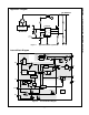
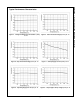
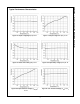
Internal Block Diagram
V
CC
ZCD
V
TH(ZCD)
V
CC
OUT
+
-
S
Q
R
Q
+
-
INV
1
5
COMP
3
Clamp
Circuit
+
-
V
CS_LIM
40k
W
8pF
4
CS
0.45
0.35
disable
2.675
2.5
disable
2.240
2.051
V
BIAS
+
-
V
Z
+
-
V
TH(S/S)
12
8.5
V
O(MAX)
V
CC
2.5V
REF
Internal
Bias
V
BIAS
V
REF
Gate
Driver
Restart
Timer
7
8
6
GND
+
-
INV_open
OVP
UVLO
RDY
2
reset
reset
H:open
Thermal
Shutdown
f
MAX
limit
V
REF
Startup without
Overshoot
V
REF
Stair
Step
Clamp
Circuit
THD
Optimized
Sawtooth
Generator
V
IN
Absent
V
CC
Control Range
Compensation
Figure 2. Functional Block Diagram