
Data Sheet

www.onsemi.com
18
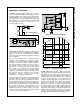
FAN7930C — Critical Conduction Mode PFC Controller
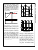
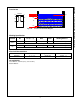
Typical Application Circuit
Application
Device
Input Voltage
Range
Rated Output
Power
Output Voltage
(Maximum Current)
LCD TV Pow er Supply
FAN7930C
90-265 V
AC
195 W
390 V (0.5 A)
Features
Average efficiency of 25%, 50%, 75%, and 100% load conditions is higher than 95% at universal input.
Pow er factor at rated load is higher than 0.98 at universal input.
Total Harmonic Distortion (THD) at rated load is low er than 15% at universal input.
Key Design Notes
When auxiliary V
CC
supply is not available, V
CC
pow er can be supplied through Zero Current Detect (ZCD)
w inding. The pow er consumption of R103 is quite high, so its pow er rating needs checking.
Because the input bias current of INV pin is almost zero, output voltage sensing resistors (R112~R115) should
be as high as possible. How ever, too-high resistance makes the node susceptible to noise. Resistor values need
to strike a balance betw een pow er consumption and noise immunity.
Quick charge diode (D106) can be eliminated if output diode inrush current capability is sufficient. Even w ithout
D106, system operation is normal due to the controller’s highly reliable protection features.
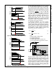
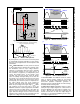
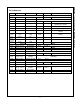
Schematic
ZNR101
,10D471
194µH, 39:5
D105
600V 8A
V
AUX
DC OUTPUT
Q101
FCPF
20N60
D106
600V 3A
FS101,
250V,5
A
R101,1M-
J
C101,
220nF
C114
,2.2n
F
LF101
,23mH
C102,
680nF
TH101
,5D15
BD101,
600V,15A
C1030,68m
F,630Vdc
C107
,33m
F
C105, 100nF
R107
,10k
C108,
220nF
C109
,47n
F
R110,10k
R109
47
R108
4.7
D103,1N414
8
D104,1N414
8
C112,470p
F
R111
0.08, 5W
C110,1n
F
R115
75k
R112
3.9M
C111
220mF, 450V
LP101,EER3019N
R113
3.9M
R114
3.9M
R104,
30k
1
7
6
8
5
2
Comp
INV
V
CC
Out
GND
ZCD
CS
RDY
4
3
C115
,2.2n
F
R103,
10k,1W
D102,
UF4004
C104,
12nF
D101,1N474
6
R102,
330k
Circuit for V
CC
. If external V
CC
is used, this circuit is not needed.
V
CC
for another power stage
Circuit for V
CC
for another power stage thus components structure and values may vary.
Optional
Figure 45. Demonstration Circuit