
Data Sheet

www.onsemi.com
17
FAN7930C — Critical Conduction Mode PFC Controller
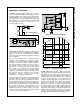
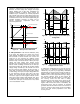
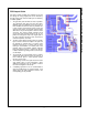
PCB Layout Guide
PFC block normally handles high sw itching current and
the voltage low energy signal path can be affected by
the high energy path. Cautious PCB layout is mandatory
for stable operation.
1. The gate drive path should be as short as possible.
The closed-loop that starts from the gate driver,
MOSFET gate, and MOSFET source to ground of
PFC controller should be as close as possible. This
is also crossing point betw een pow er ground and
signal ground. Pow er ground path from the bridge
diode to the output bulk capacitor should be short
and w ide. The sharing position betw een pow er
ground and signal ground should be only at one
position to avoid ground loop noise. Signal path of
the PFC controller should be short and w ide for
external components to contact.
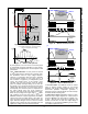
2. The PFC output voltage sensing resistor is normally
high to reduce current consumption. This path can
be affected by external noise. To reduce noise
potential at the INV pin, a shorter path for output
sensing is recommended. If a shorter path is not
possible, place some dividing resistors betw een
PFC output and the INV pin — closer to the INV pin
is better. Relative high voltage close to the INV pin
can be helpful.
3. The ZCD path is recommended close to auxiliary
w inding from boost inductor and to the ZCD pin. If
that is difficult, place a s mall capacitor (below
50 pF) to reduce noise.
4. The sw itching current sense path should not share
w ith another path to avoid interference. Some
additional components may be needed to reduce
the noise level applied to the CS pin.
5. A stabilizing capacitor for V
CC
is recommended as
close as possible to the V
CC
and ground pins. If it is
difficult, place the SMD capacitor as close to the
corresponding pins as possible.
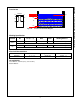
Figure 44. Recommended PCB Layout