
Data Sheet

www.onsemi.com
15
FAN7930C — Critical Conduction Mode PFC Controller
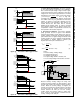
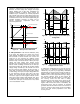
which is normally higher than in normal operation. This
operation is improved w hen soft-start time is very long.
How ever, too much startup time enlarges the output
voltage building time at light load. FA N7930C has
overshoot protection at startup. During startup, the
feedback loop is controlled by an internal proportional
gain controller and, w hen the output voltage reaches the
rated value, it sw itches to an external compensator after
a transition time of 30 ms. This internal proportional gain
controller eliminates overshoot at startup and an
external conventional compensator takes over
successfully afterw ard.
Depends on Load
V
OUT
V
COMP
Startup Overshoot
Internal Controller
t
Conventional Controller
Startup Overshoot Control
Control Transition
Figure 37. Startup without Overshoot
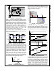
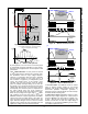
9. THD Optimization: Total Harmonic Distortion (THD)
is the factor that dictates how closely input current
shape matches sinusoidal form. The turn-on time of the
PFC controller is almost constant over one AC line
period due to the extremely low feedback control
response. The turn-off time is determined by the current
decrease slope of the boost inductor made by the input
voltage and output voltage. Once inductor current
becomes zero, resonance betw een C
OSS
and the boost
inductor makes oscillating w aveforms at the drain pin
and auxiliary w inding. By checking the aux iliary w inding
voltage through the ZCD pin, the controller can check
the zero current of boost inductor. At the same time, a
minor delay is inserted to determine the valley position
of drain voltage. The input and output voltage difference
is at its maximum at the zero cross point of AC input
voltage. The current decrease slope is steep near the
zero cross region and more negative inductor current
flow s during a drain voltage valley detection time. Such
a negative inductor current cancels dow n the positive
current flow s and input current becomes zero, called
“zero-cross distortion” in PFC.
1.5V
150ns
1.4V
ON
V
ZCD
t
I
INDUCTOR
MOSFET gate
I
NEGATIVE
ON
I
IN
I
MOSFET
I
DIODE
Figure 38. Input and Output Current Near Input
Voltage Peak
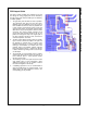
1.5V
150ns
1.4V
ON
ON
V
ZCD
t
I
INDUCTOR
MOSFET gate
I
NEGATIVE
ON ON
I
IN
Figure 39. Input and Output Current Near Input
Voltage Peak Zero Cross
To improve this, lengthened turn-on time near the zero
cross region is a w ell-know n technique, though the
method may vary and may be proprietary. FAN7930C
optimizes this by sourcing current through the ZCD pin.
Auxiliary w inding voltage becomes negative w hen the
MOSFET turns on and is proportional to input voltage.
The negative clamping circuit of ZCD outputs the
current to maintain the ZCD voltage at a fixed value.
The sourcing current from the ZCD is directly
proportional to the input voltage. Some portion of this
current is applied to the internal saw tooth generator,
together w ith a fixed-current source. Theoretically, the
fixed-current source and the capacitor at saw tooth
generator determine the maximum turn-on time w hen no
current is sourcing at ZCD c lamp circuit and available
turn-on time gets shorter proportional to the ZCD
sourcing current.