
Data Sheet

www.onsemi.com
14
FAN7930C — Critical Conduction Mode PFC Controller
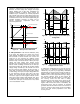
V
OUT
PFC
+
-
INV
1
COMP
3
Clamp
Circuit
+
-
V
REF
Stair
Step
THD-Optimized
Sawtooth
Generator
Sawtooth
MOSFET Off
R1
C1
C2
1V
6.2V
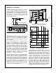
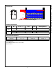
Figure 32. Control Circuit
Unlike a conventional voltage-mode PWM controller,
FA N7930C turns on the MOSFET at the falling edge of
ZCD signal. The “ ON” instant is determined by the
external signal and the turn-on time lasts until the error
amplifier output (V
COMP
) and saw tooth w aveform meet.
When load is heavy, output voltage decreases, scaled
output decreases, COMP voltage increases to
compensate low output, turn-on time lengthens to give
more inductor turn-on time, and increased inductor
current raises the output voltage. This is how a PFC
negative feedback controller regulates output.
The maximum of V
COMP
is limited to 6.5 V, w hich
dictates the maximum turn-on time. Sw itching stops
w hen V
COMP
is low er than 1.0 V.
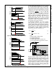
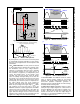
ZCD
after COMPARATOR
V
COMP
& Sawtooth
MOSFET gate
t
s/V155.0
Figure 33. Turn-On Time Determination
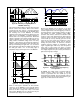
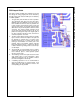
The roles of PFC controller are regulating output voltage
and input current shaping to increase pow er factor. Duty
control based on the output voltage should be fast
enough to compensate output voltage dip or overshoot.
For the pow er factor, how ever, the control loop must not
react to the fluctuating A C input voltage. These tw o
requirements conflict; therefore, w hen designing a
feedback loop, the feedback loop should be least ten
times slow er than AC line frequency. That slow
response is made by C1 at the compensator. R1 makes
gain boost around operation region and C2 attenuates
gain at higher frequency. Boost gain by R1 helps raise
the response time and improves phase margin.
Freq.
C
1
R
1
Proportional
gain
C
2
Integrator
High-Frequency
Noise Filter
Gain
Figure 34. Compensators Gain Curve
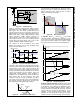
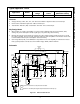
For the transconductance error amplifier side, gain
changes based on differential input. When the error is
large, gain is large to suppress the output dip or peak
quickly. When the error is small, low gain is used to
improve pow er factor performance.
I
COMP
SourcingSinking
Powering
Braking
2.5V
2.4V
2.6V
mho250
mho115
Figure 35. Gain Characteristic
7. Soft-Start: When V
CC
reaches V
START
, the internal
reference voltage is increased like a stair step for 5 ms.
As a result, V
COMP
is also raised gradually and MOSFET
turn-on time increases smoothly. This reduces voltage
and current stress on the pow er sw itch during startup.
V
REF
SS
g
M
V
INV
=0.4V
I
SOURCE
COMP
V
COMP
I
SOURCE
COMP
R
COMP
=V
COMP
t
(V
REF
SS
-V
INV
)
g
M
=I
SOURCE
COMP
V
REF
END
=2.5V
5ms
V
CC
V
START
=12V
Figure 36. Soft-Start Sequence
8. Startup without Overshoot: Feedback control speed
of PFC is quite slow . Due to the slow response, there is
a gap betw een output voltage and feedback control.
That is w hy over-voltage protection (OV P) is critical at
the PFC controller and voltage dip caused by fast load
changes from light to heavy is diminished by a bulk
capacitor. OVP is triggered during startup phase.
Operation on and off by OV P at startup may cause
audible noise and can increase voltage stress at startup,